
Click the blue text
Follow us
1. Principle
The SPI (Serial Peripheral Interface) protocol is a high-speed, efficient, full-duplex communication bus that allows the CPU to perform synchronous serial data transmission with low-speed peripheral devices. It mainly uses a synchronous clock signal to simultaneously send and receive serial data, thus achieving full-duplex communication. It is commonly used for short-distance communication, primarily in embedded systems.
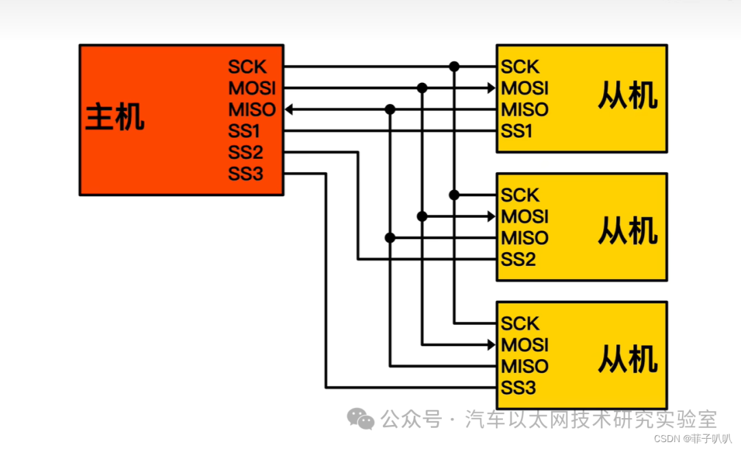
1. SPI Wiring
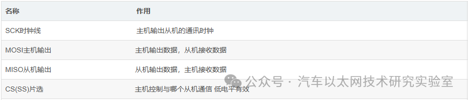
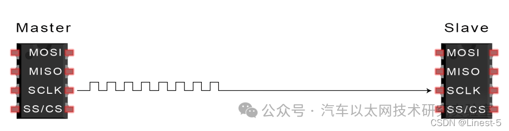
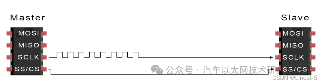
The SPI interface occupies only four lines inside the chip, which mainly include two data lines, one chip select line, and one clock signal line. These four lines correspond to the four types of signals during SPI protocol transmission, which are:
Master Output Signal ———-> MOSI
Slave Input Signal ———-> MISO
Chip Select Signal —————> CS (SS)
Clock Signal —————> SCK
The SPI protocol defines two working modes: master mode and slave mode. The module operating in master mode is the master, while the module operating in slave mode is the slave. Data exchange between the master and slave occurs according to the SPI timing.
A typical SPI system should include only one master and one or more slaves. The following diagram illustrates a master-slave configuration:
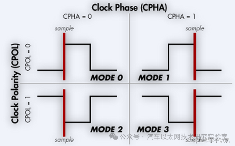
2. Polarity (CPOL) and Phase (CPHA)
The SPI phase and polarity refer to the characteristics of the clock signal in SPI communication. The clock signal is generated by the master to control the synchronization of data exchange between the master and slave devices.
The clock polarity determines the clock level when the bus is idle.
The clock phase determines whether the data is sampled on the rising or falling edge of the clock.
Reading different SPI devices may require different clock polarity and phase settings to ensure correct communication.
(1) Polarity
Indicates whether the clock SCK is at a low level “0” or a high level “1” when idle.
CPOL=0 means the clock is low when idle, so when SCK is active, it is high.
CPOL=1 means the clock is high when idle, so when SCK is active, it is low.
(2) Phase
Corresponds to whether data is sampled on the first or second edge.
0 corresponds to the first edge.
1 corresponds to the second edge.
(3) Polarity and Phase Combinations
For: CPHA=0, indicating the first edge:
-
For CPOL=0, the idle state is low, and the first edge is from low to high, so it is the rising edge;
-
For CPOL=1, the idle state is high, and the first edge is from high to low, so it is the falling edge;
CPHA=1 indicates the second edge:
-
For CPOL=0, the idle state is low, and the second edge is from high to low, so it is the falling edge;
-
For CPOL=1, the idle state is high, and the first edge is from low to high, so it is the rising edge;
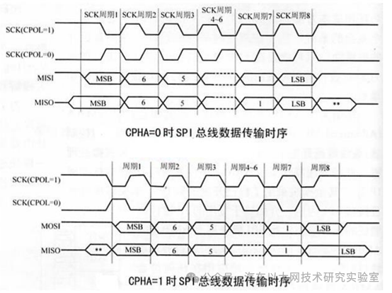
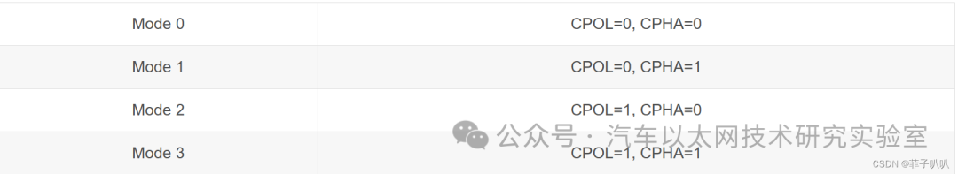
The corresponding four combinations are:
Reference code for the four modes:
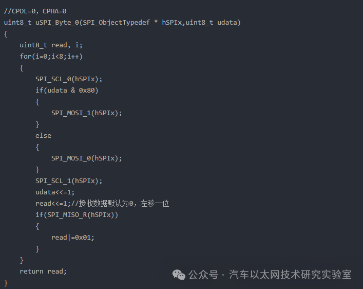
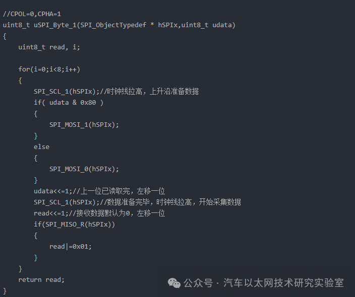
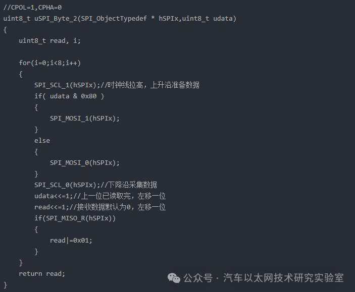
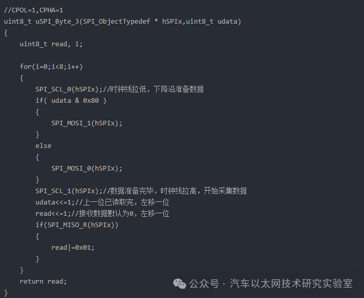
Of course, the specific collection method to be used needs to be referenced in our chip manual.
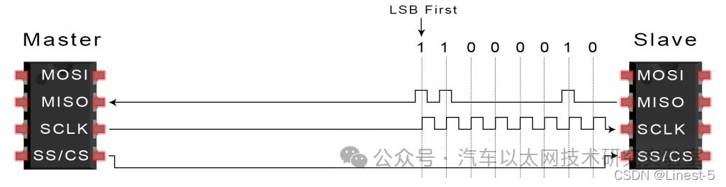
2. Communication Process
Unlike IIC, SPI does not require a start signal or an end signal; data can be transmitted directly by pulling down a certain chip select signal to select the connected slave device.
1. The master outputs the clock signal
2. Connect to the slave device
The master switches the SS/CS pin to a low state to activate the slave:
3. The master sends data
The master sends data to the slave one bit at a time along the MOSI line. The slave reads the received bits: the high bit is read first.
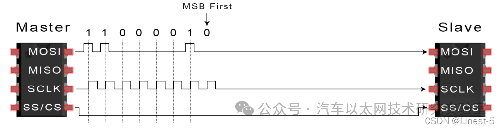
4. Slave response
If a response is needed, the slave returns data to the master one bit at a time along the MISO line. The master reads the bits as they are received: the low bit is read first.
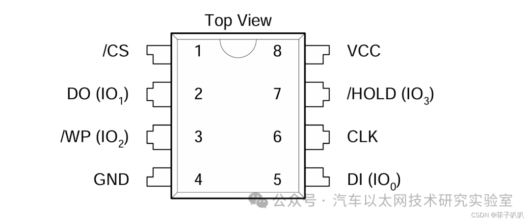
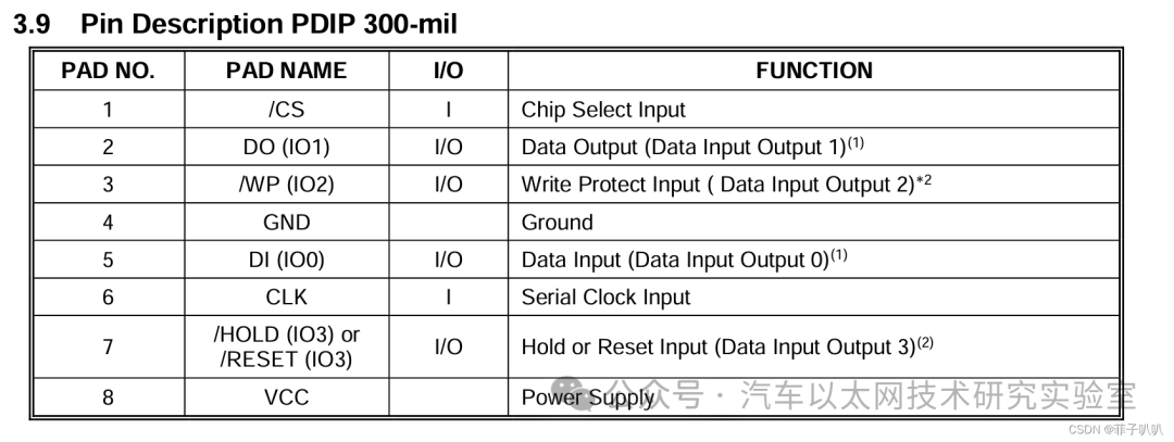
3. Flash Chip —- W25QXX
The W25QXX is a FLASH storage chip produced by Winbond. This chip supports a voltage range of 2.7V-3.6V.
1. Pins
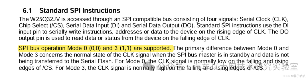
2. Polarity and Phase Modes
According to the specification manual, we can see that:
The W25QXX SPI transmission supports mode 0 and mode 3, that is:
Mode 0 (CPOL=0, CPHA=0)
Mode 3 (CPOL=1, CPHA=1).
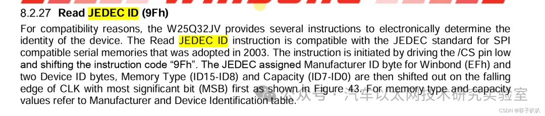
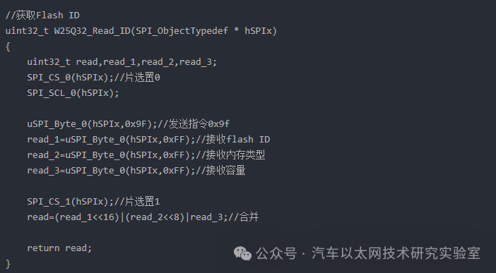
3. Obtaining the Chip’s Flash ID
Once the circuit is built and the basic SPI communication functions are written, the next step is to obtain a value returned by the chip to test whether the circuit and basic functions are successful.
According to its specification manual, there are two points to note before obtaining the ID: 1. MSB is transmitted first, 2. The CS must be pulled low during the operation.
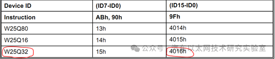
The ID numbers vary by model.
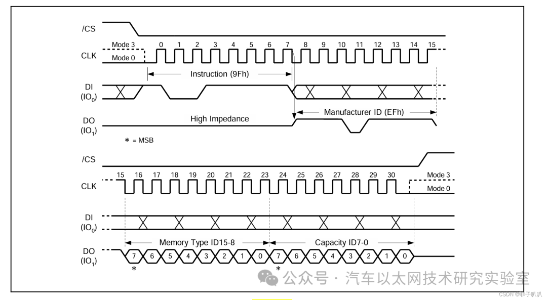
According to the timing diagram below:
-
To obtain the ID, CS must be low, and the high bit is transmitted first.
-
The command to obtain the ID is 0x90.
-
The received information consists of three bytes: the first byte is the Manufacturer ID (fixed value 0xEF), the second byte is the Memory Type, and the third byte is the Capacity.
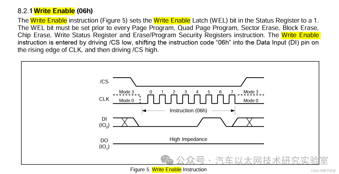
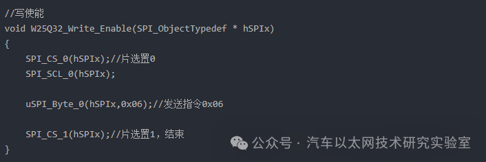
4. Chip Write Enable
The write enable operation is similar to the read ID operation, with the command being 0x06. After successful write enable, the S1 bit of Status Register1 (WSL) is set to 1, allowing write and erase operations.
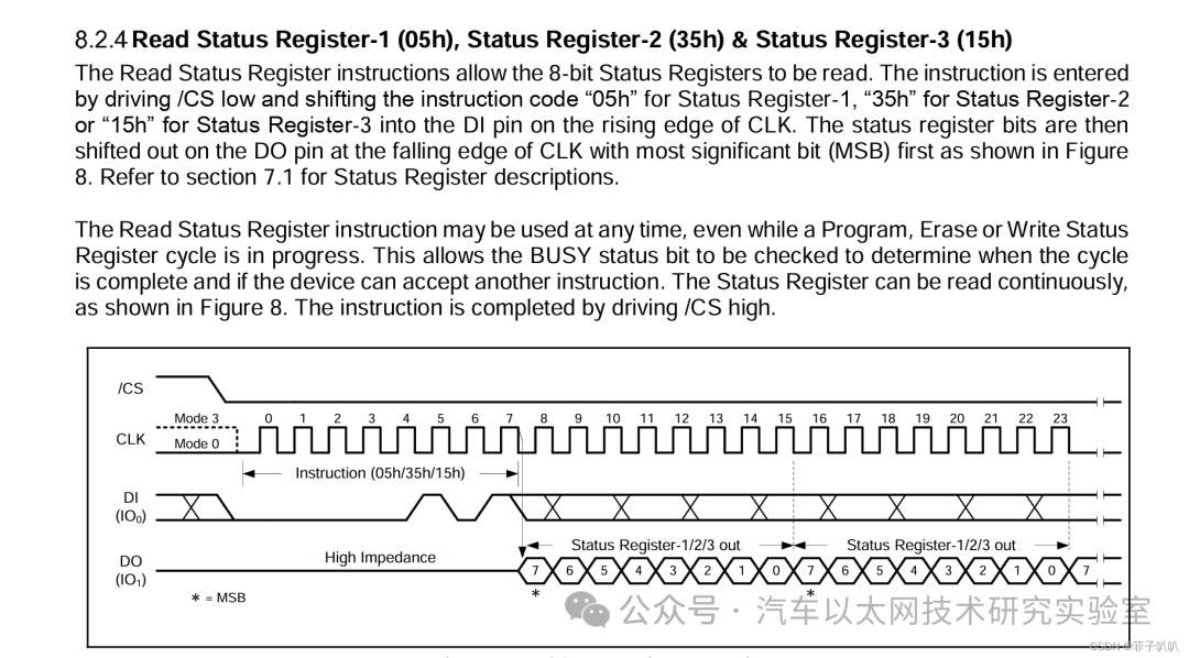
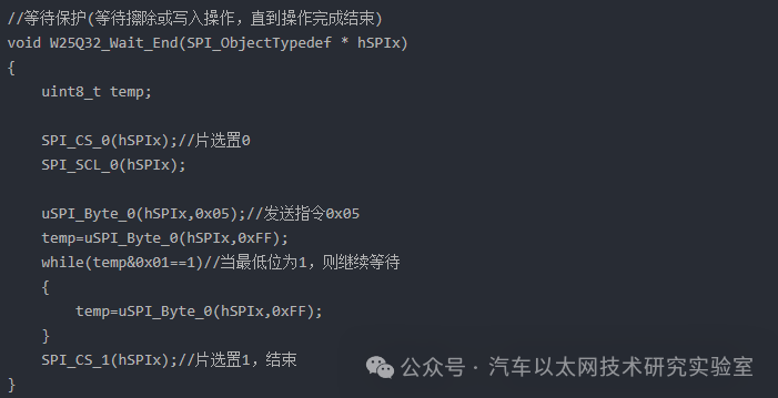
5. Busy Wait Operation
When the chip is performing erase or write operations, no other operations are allowed. It must enter a wait state until the operation is completed, at which point the S0 bit of Status Register1 (BUSY) is reset to 0, allowing subsequent operations. The function must continuously read the status register to extract the S0 data to determine the status of the corresponding operation. The command to read Status Register1 is 0x05, and the reading method is MSB, so the S0 bit corresponds to the operation bit 0x01, similar to the read ID operation.
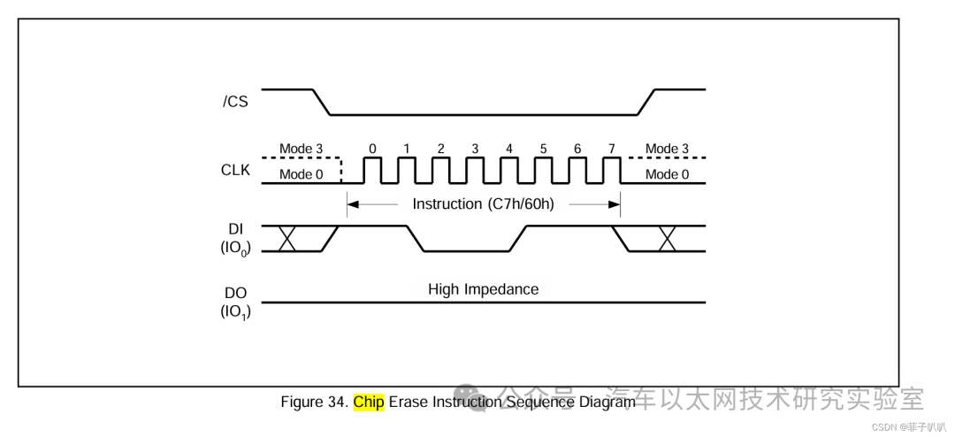
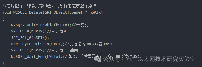
6. Erase Command
The W25Q32 is a non-volatile memory, and before writing data, an erase operation must be performed.
-
The so-called chip erase fills the storage unit bytes with 0xFF, which is the erase operation.
-
Before the chip erase operation, Write Enable must be enabled, as previously mentioned.
-
The command for chip erase operation is 0x07 or 0x60, and CS must also be low.
-
After the chip erase operation is completed, a waiting period is required (read busy status), as previously mentioned.
-
Other operations are similar to the read ID operation.
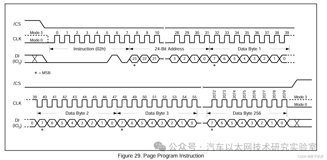
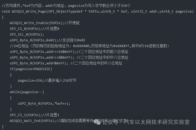
7. Page Write Operation
The maximum write unit for W25Qxx is a page, with a maximum of 256 bytes per page. If more than 256 bytes need to be written, a new page must be written. Each 16 pages form a sector, and each 16 sectors form a block. The W25Q32 has a capacity of 4MB, with a total of 64 blocks, 1024 sectors, and 16384 pages. The address range is (0x000000-0x2FFFFF), theoretically, each address bit corresponds to one byte. In practice, when continuously writing large data, the capacity issues of pages, sectors, and blocks must also be considered. Note that before writing, it must be ensured that an erase operation has been performed; the minimum erase unit is not a page but a sector.
1 block = 16 sectors, 1 sector = 16 pages, 1 page = 256 bytes
-
Page write operations are similar to erase operations, requiring CS to be low, write enable, and busy wait.
-
The page write operation command is 0x02, followed by a 24-bit address (the starting address of each page is: 0xXXXX00, the ending address is 0xXXXXFF, where X is any hexadecimal number).
-
After completing the write address, write data content not exceeding 256 bytes.
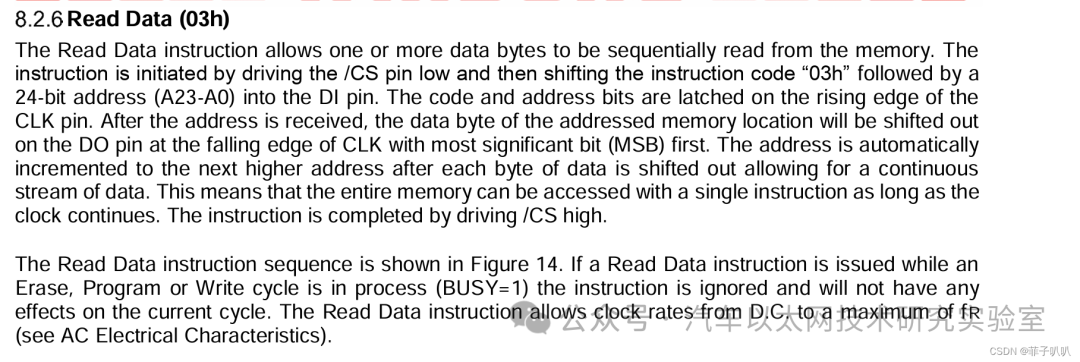
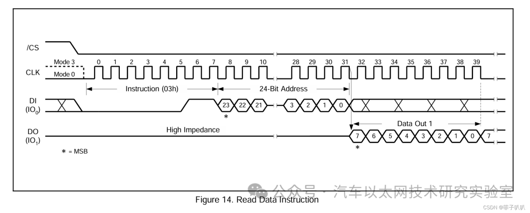
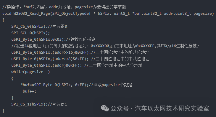
8. Read Operation
The read operation is relatively simple compared to the write operation, as it does not require consideration of pages, sectors, or blocks; a 24-bit address is sufficient for reading.
-
The read operation is similar to the read ID operation, requiring CS to be low.
-
The read operation command is 0x03, followed by a 24-bit address.
-
After completing the write address, directly read the data content.
9. Demo
Write 0x01, 0x02, 0x03, 0x04, 0x05 starting from address 00 to the W25Q32 and read the data from address 00-05, sending it to the computer via serial port.
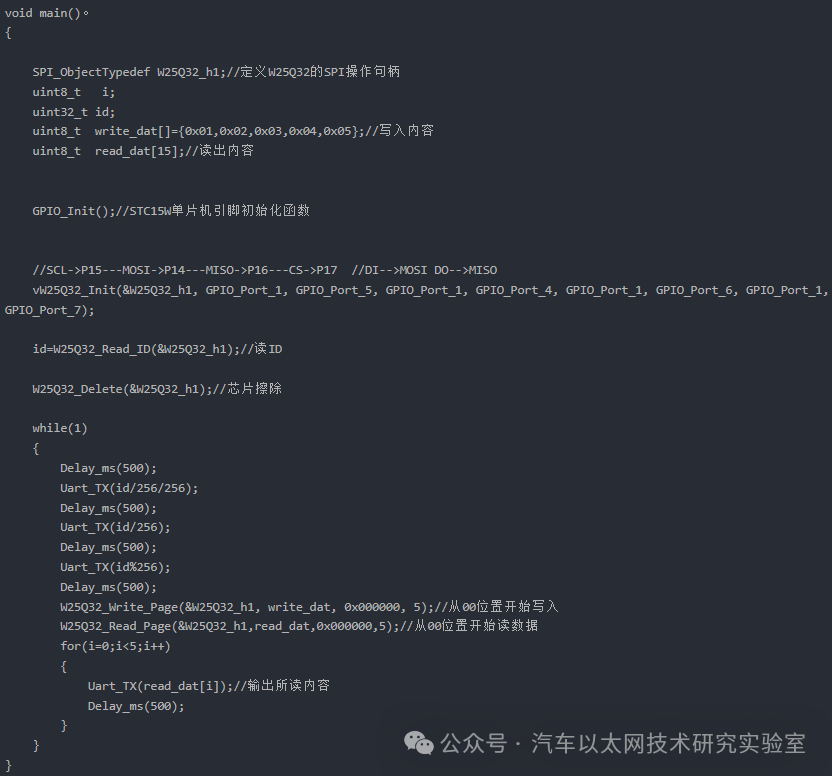
All information is sent to the computer via the serial port.
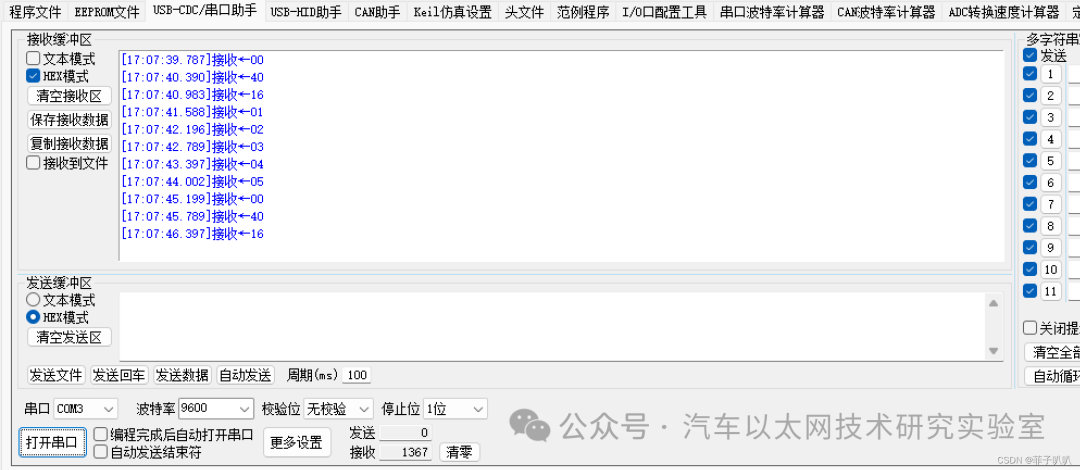
The first three sent data are the W25Q32 chip information, and the next five data are the data stored in that memory.


*Disclaimer: This article is original or forwarded by the author. If it inadvertently infringes on any party’s intellectual property rights, please inform us for deletion.The above images and text are sourced from the internet; if there is any infringement, please contact us in a timely manner, and we will delete it within 24 hours.The content of the article represents the author’s personal views, and the Automotive Ethernet Technology Research Laboratory reprints it only to convey a different perspective, not representing the Automotive Ethernet Technology Research Laboratory’s endorsement or support of that view. If there are any objections, please feel free to contact the Automotive Ethernet Technology Research Laboratory.
Original link:
https://blog.csdn.net/m0_73409202/article/details/137008620