1. Abstract This design selects the STM32F103C8T6 microcontroller chip as the core processor of the system and employs a closed-loop PID control strategy to develop a high-efficiency BOOST boost converter system. The hardware components include the STM32F103C8T6 microcontroller control circuit module, auxiliary power circuit module, main power boost module, and current and voltage acquisition circuit module. The microcontroller outputs a PWM signal to the EG2104 chip to control the switching of the MOSFETs with complementary PWM signals. The system provides feedback on the output through voltage and current sampling circuits, and after sampling via the A/D converter, the data is transmitted to the microcontroller control circuit, forming a closed-loop control system that ensures the output voltage and current remain stable at the set target values.2. System Scheme Principles and Analysis1. BOOST Circuit Topology
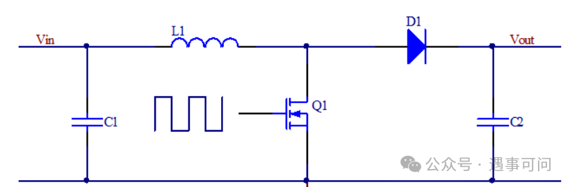
The following is the topology of the BOOST circuit, with the main components being one MOSFET, one inductor, one diode, and a capacitor. The MOSFET is controlled by PWM to turn on and off.
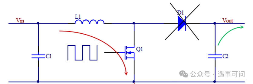
When the MOSFET is turned on, the current flows as indicated by the red arrows in the figure below, and the inductor begins to charge, converting energy into magnetic energy. At this time, the diode is reverse-biased and all output energy is provided by the capacitor C2, as indicated by the green arrows.
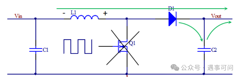
 After the MOSFET is turned off, the current flows as indicated by the green arrows in the figure below, and the inductor releases energy. At this time, the inductor acts like a battery, supplying power to the load in series with Vin, while charging the output capacitor C2. The load is powered by the output capacitor C2 and the diode D1. D1 is generally chosen to be a Schottky diode with fast conduction and low forward voltage drop.
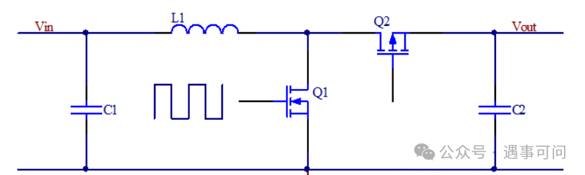
 The above circuit topology has a flaw: when the circuit is not working, the input voltage flows through the inductor L1 and diode D1 to the load, which can sometimes cause unwanted power loss, necessitating the addition of a switch circuit. To solve this problem, we can choose a synchronous type chip. The following is the topology of a synchronous BOOST boost circuit, where the diode is replaced with a MOSFET, which is controlled by internal logic of the chip. When the chip is not working, the MOSFET is turned off, thus preventing leakage issues. The MOSFET has a lower conduction voltage drop and lower power loss, making it more efficient than a diode.
 2. PI Algorithm and Parameter Adjustment Method Proportional-Integral-Derivative (PID) algorithms are mostly used in industrial control, with approximately 95% of industrial automation closed-loop systems utilizing PID algorithms.PID control strategy integrates proportional, integral, and derivative control actions to form a closed-loop feedback control. Before the advent of MCU, PID was implemented using analog electronic components. Now, almost all PID control utilizes MCU for data computation and control.Due to its adaptability and reliability, PID has been traditionally applied in process control[16].PID algorithms combine the error signal generated by the circuit into total control through linear combinations of proportional, integral, and derivative parts, thus providing feedback control of the circuit’s errors.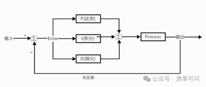
PID controllers are popular due to their mature technology, ease of learning and operation, no need for complex mathematical models, and excellent control effects.PID algorithms can be divided into P algorithms, PI algorithms, PD algorithms, and PID algorithms.P algorithms react immediately to any error, adjusting the control quantity to reduce the error.P algorithm’s control strength is determined by the proportional coefficient KP, with a larger KP value resulting in stronger control, but excessively high KP values may lead to system instability.
Integral control treats the accumulation of errors as output. When there is an error signal in the circuit, its output continuously increases. When the error e(t) is zero, the output u(t) will stabilize at a certain value, thus maintaining the system at the set value r(t) and achieving a stable state. Although the integral part can eliminate static errors, it can reduce the system’s operating speed and increase overshoot.TI values that are higher will have a smaller cumulative effect.Increasing the integral time constant TI will slow down the elimination of static errors, enhancing system stability and reducing overshoot. Therefore, the TI value must be set according to actual needs.
The derivative part can suppress changes in errors, adjusting based on the rate of change of the error generated in the circuit. The greater the change in error, the higher its output, allowing for control adjustments before the error increases. Derivative control can reduce overshoot and restrain system aggressiveness, making the system more stable.However, the derivative control part is very sensitive to input signal noise, so it should not be used independently in high-noise scenarios. Properly setting the derivative constant ( TD) can enhance derivative control adjustments, optimizing the circuit’s operational performance.Considering all factors, the PI algorithm is most suitable for the feedback control requirements of this system design.
3. System Scheme Design
The MOSFET driver circuit uses the EG2104 chip with built-in dead time, monitoring current with the INA282 chip for current loop feedback control, while employing a differential operational amplifier circuit for output voltage acquisition to achieve voltage loop feedback control. By sampling voltage and current and using the PI algorithm, boost, constant voltage, and constant current are realized.
3.1 Boost Circuit Module The boost circuit module consists of power circuits, driver circuits, and three-phase inverter half-bridge circuits, which is the core part of whether the system can boost the voltage. The boost circuit module is controlled by PWM output from the microcontroller. The driver circuit outputs complementary PWM control for switching the MOSFETs, and also protects the MOSFETs from large current surges. In this system, the boost circuit part has a maximum output voltage of 60V, with a maximum current of 4A.
3.2 MCU Control Circuit Module
The microcontroller control circuit is the core that ensures the system operates normally. It consists of the basic system circuit, STM32F103C8T6 chip, OLED display circuit, key input circuit, analog-to-digital conversion circuit, LED indicator circuit, and pulse width modulation circuit. The output of the pulse width modulation circuit is directly used to control the BOOST circuit module. The voltage feedback collected by the AD converter pins is sent to the voltage and current acquisition modules to control the voltage output and current of the BOOST circuit part.
3.3 Auxiliary Power Circuit Module
The auxiliary power circuit module supplies power to various circuit module chips in the microgrid simulation system, stepping down the 20V DC voltage through the SCT2A10 to 5V for powering each circuit module chip.
4. Implementation of BOOST Boost System
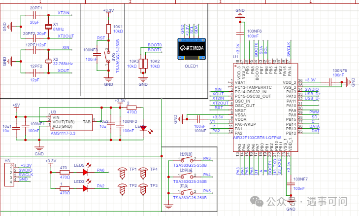
The key component of the system design is the STM32F103C8T6 microcontroller control circuit module. The STM32F103C8T6 microcontroller control circuit module includes an oscillator circuit, power supply circuit, reset logic circuit, bootloader circuit, key input interface, OLED display module, LED indicator circuit, ADC circuit, and PWM circuit, ensuring the stable operation and flexible control capability of the system.
The STM32F103C8T6 microcontroller is a high-performance 32 bit ARM Cortex™-M4 core, with a working frequency of up to 8 MHz. The working voltage range is 2.0V to 3.6V, with each peripheral device equipped with independent clock control, reducing energy consumption by managing these control switches.
4.1 BOOST Circuit Design
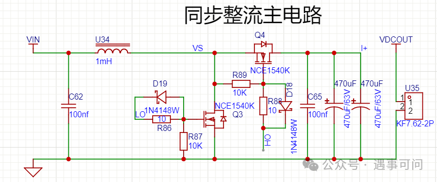
Capacitor selection is based on empirical values, with input capacitors of 470UF/63V and output capacitors of 470UF/63V connected in parallel. The input capacitor can be slightly smaller; I used whatever capacitors I had on hand. Charging the input capacitor protects the MOSFET from large current surges. The output capacitor stores energy and filters, resulting in perfect DC.
NCE1540K has a voltage rating of 150V, and the maximum output DC voltage of the system is 60V. This is critical for the stable operation of the system. The maximum output current of the system is 4A, while NCE1540K can handle a maximum current of 40A. The selected MOSFET is NCE1540K. I only have MOSFETs from NCE, and they seem to be quite standard. If you want to improve efficiency and performance, I recommend switching to better MOSFETs, as this MOSFET gets quite hot at 150W.
To adjust the rise and fall times of the control pulses, prevent oscillation, and reduce the impact voltage at the drain of the switching tube, this can be achieved by reducing the series resistance at the gate of the switching tube. The resistance used in this system design is 10Ω, and a diode is connected in reverse across the gate circuit to improve the discharge speed of the gate. The model used in this system is 1N4148. A 10kΩ resistor is added between the gate and drain of the MOSFET to help reduce the static leakage current generated during the MOSFET’s turn-off process.
The driver circuit separates the MOSFET switch and the microcontroller control chip, protecting the microcontroller control chip from burning out, which would cause the system to fail to operate. The EG2104 is a cost-effective gate driver chip suitable for MOSFETs and IGBTs with SD functionality. The EG2104 chip operates within a voltage range of 2.8V to 20V, with a static power consumption of less than 1uA. From the above description, it can fully meet the requirements of the topic.
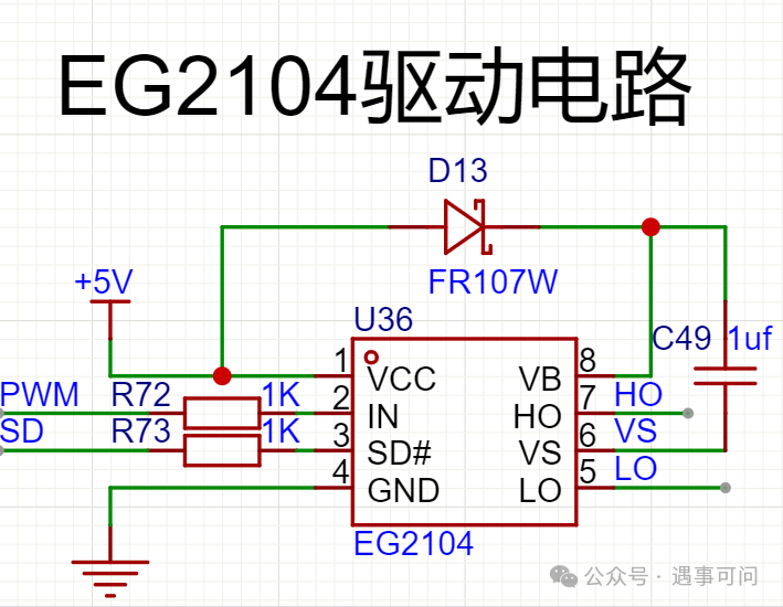
There is a direct proportional relationship between the losses of the MOSFET and the switching frequency. After comprehensive consideration, the switching frequency of the three-phase inverter circuit module designed in this system is set to 20 kHz. You can also try increasing the switching frequency.
4.2 Voltage and Current Sampling Circuit Design
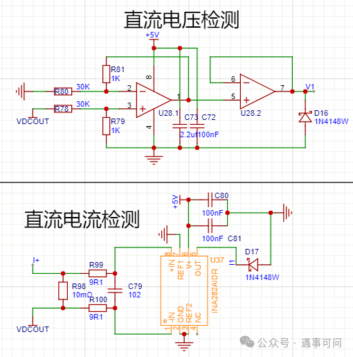
The system uses a differential amplifier circuit to collect voltage values and the INA282 to collect current values, transmitting them to the microcontroller control circuit for feedback adjustment. Assuming the output voltage is 60V, after R78 and R79 voltage division, the output voltage through a voltage follower is 60/(1/30)=2V, allowing the microcontroller to detect the magnitude of the output voltage. Changing the resistance values of R78 and R79 can alter the scaling factor. Current detection is performed using the INA282 chip, which I selected with a gain of 50. Assuming the output current is 4A, the output current is 0.01*50*4=2V, allowing the microcontroller to detect the constant current output. Here, 0.01 is the current sampling resistor R98.
4.3 Auxiliary Power Circuit Design
The SCT2A10 chip steps down the 20V input voltage through BUCK to output a 5V power supply. The SCT2A10 has a power supply range of 4.5V to 100V with a maximum output of 600mA, and it can adjust the switching frequency. The chip is designed with over-voltage and over-current protection functions. The typical internal reference voltage for the FB voltage is 0.8V. Here, R1=120KΩ, VREF=0.8V, R2=22KΩ, and the calculated VOUT=5.1V. 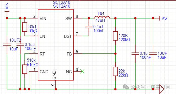
5. Software Program Design
The main program primarily initializes the BOOST circuit system and calls subroutines. After all configuration and initialization steps are completed, the program enters a While loop, waiting for a timer interrupt to trigger. In the timer interrupt handler, voltage signal sampling is performed, followed by PID algorithm calculations, and then control of the voltage and current loops.
5.1. PID Control Program Design
The PID algorithm program of the system design is a crucial part of the entire control function. The selection of the PID algorithm and the adjustment of parameters play a key role in the response speed and stable operation of the system. The microcontroller chip’s ADC function uses the voltage values collected by the differential operational amplifier as a reference for control through the PID algorithm, with the microcontroller chip outputting corresponding values to achieve constant voltage. The microcontroller chip’s ADC function uses the voltage values collected by the INA282 chip as output for PID algorithm control, with the microcontroller chip outputting corresponding values to achieve constant current. The above describes a dual closed-loop control strategy, including a voltage outer loop P controller and a current inner loop PID controller, which are responsible for regulating output voltage and current, respectively.
6. Test Results and Analysis
6.1 Constant Voltage Test
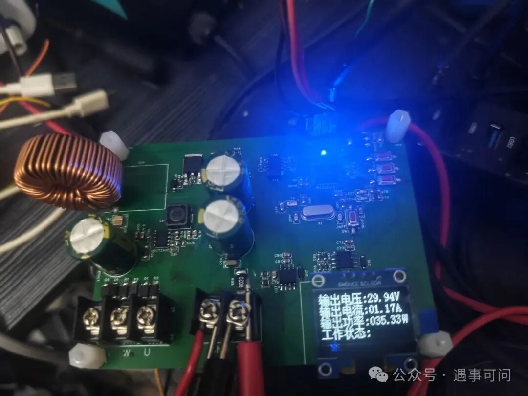
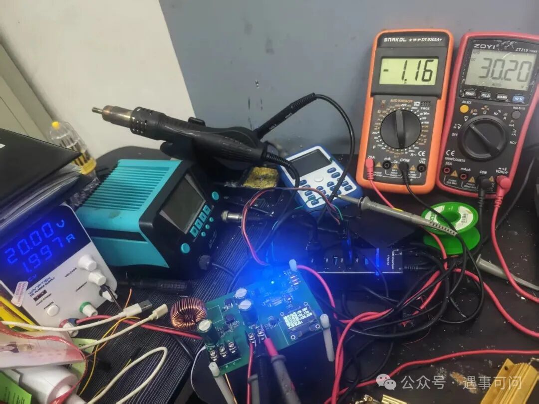
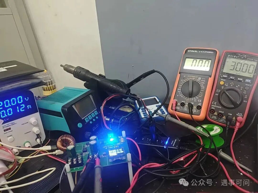
Input 20V, output 30V, calculated efficiency is 88%, which is not very high. The load adjustment rate is 0.7%. Areas for improvement include replacing the MOSFET with a higher performance one and increasing the output frequency of the microcontroller. The output capacitor’s capacity can be reduced; I used two 470uF capacitors in parallel.
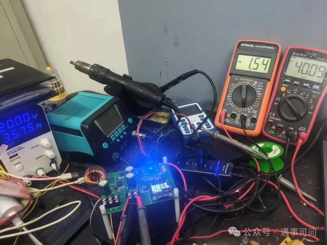
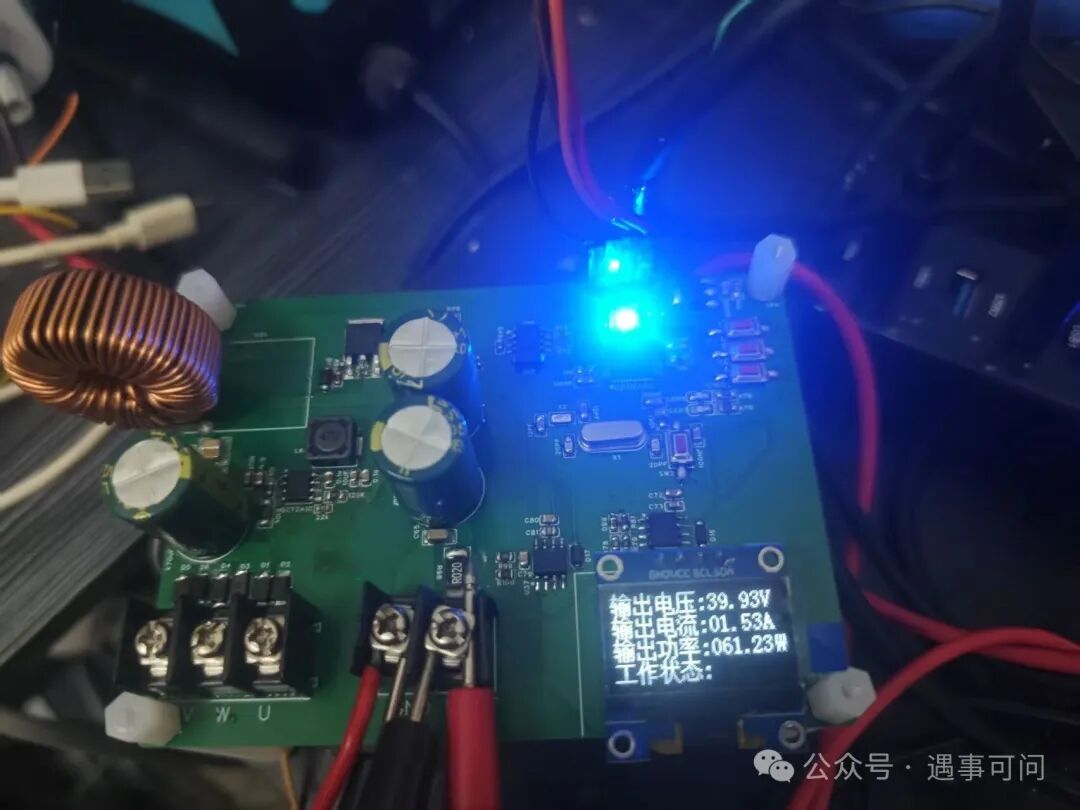
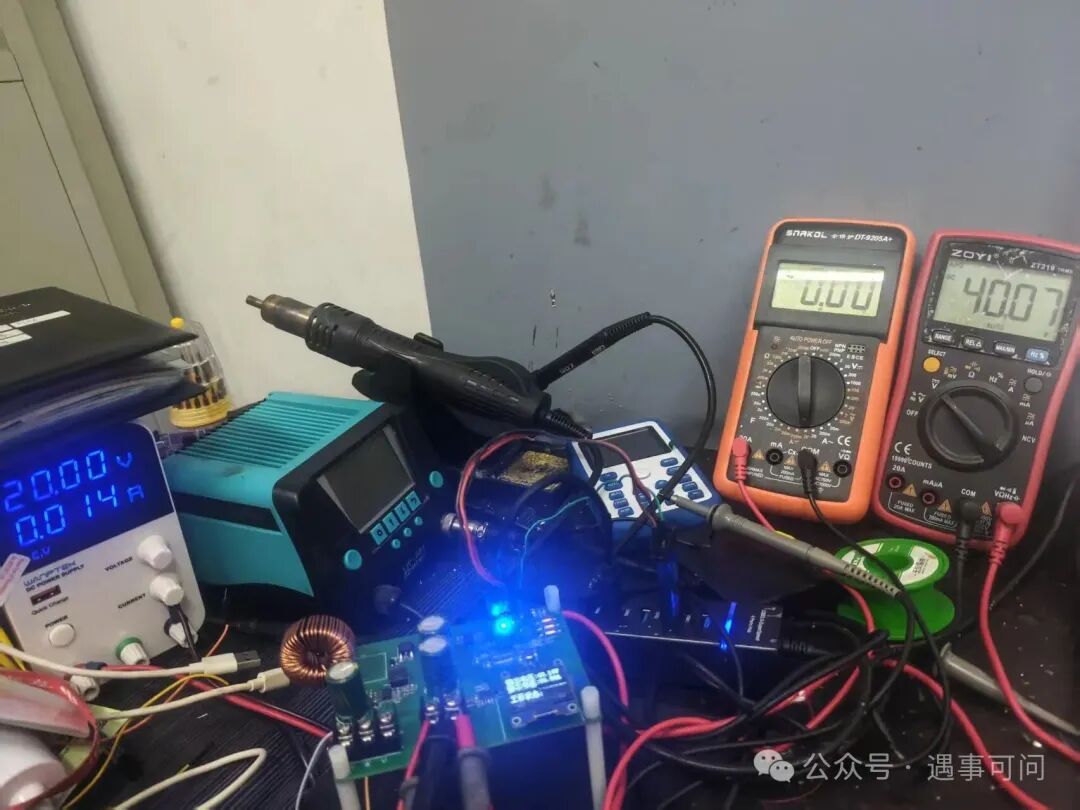
Input 20V, output 40V, calculated efficiency is 86%, which is not very high. The load adjustment rate is 0.05%. Areas for improvement include replacing the MOSFET with a higher performance one and increasing the output frequency of the microcontroller. The output capacitor’s capacity can be reduced; I used two 470uF capacitors in parallel.
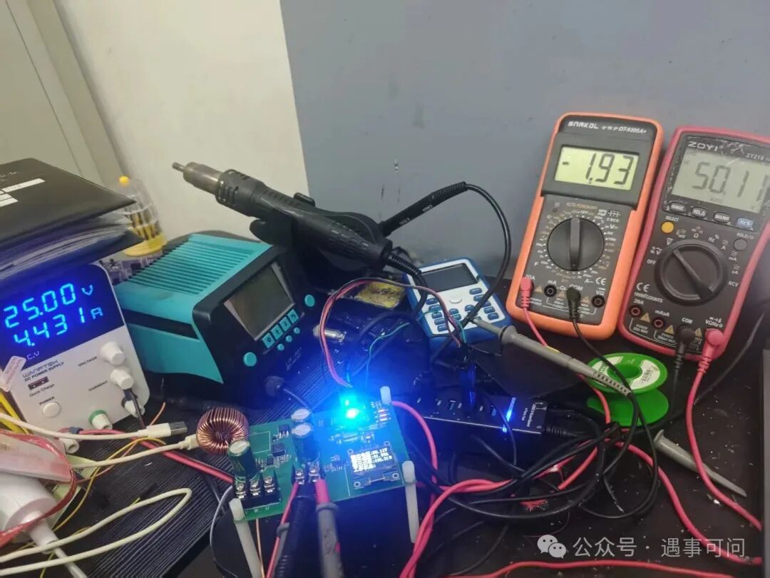
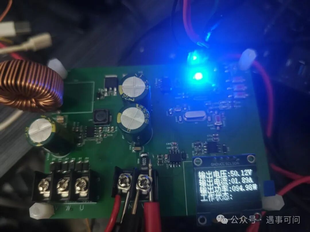
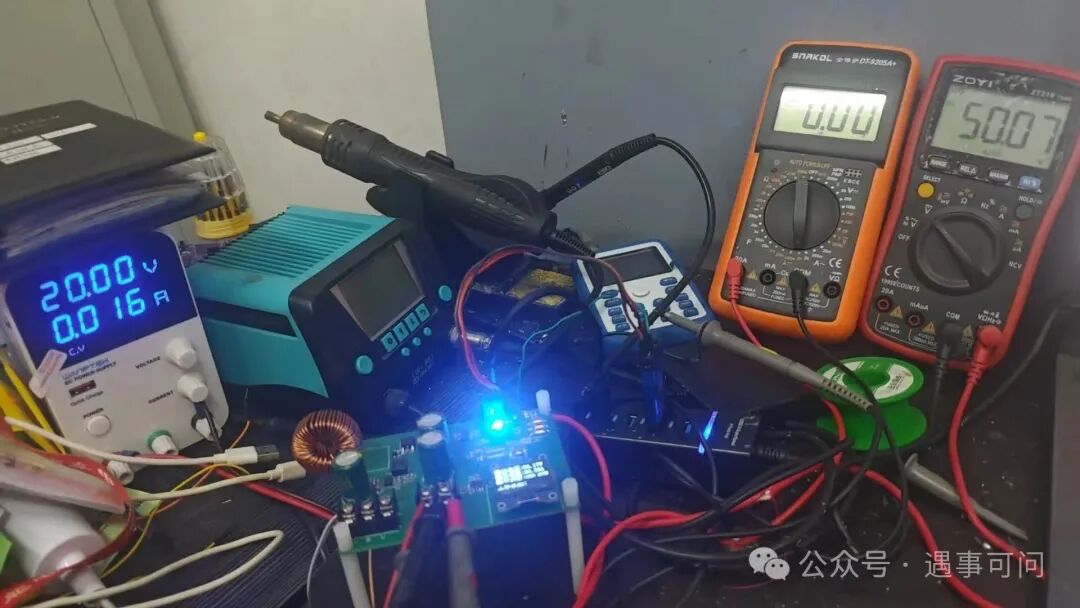 Input 25V, output 50V, calculated efficiency is 88%, which is not very high. The load adjustment rate is 0.08%. Areas for improvement include replacing the MOSFET with a higher performance one and increasing the output frequency of the microcontroller. The output capacitor’s capacity can be reduced; I used two 470uF capacitors in parallel.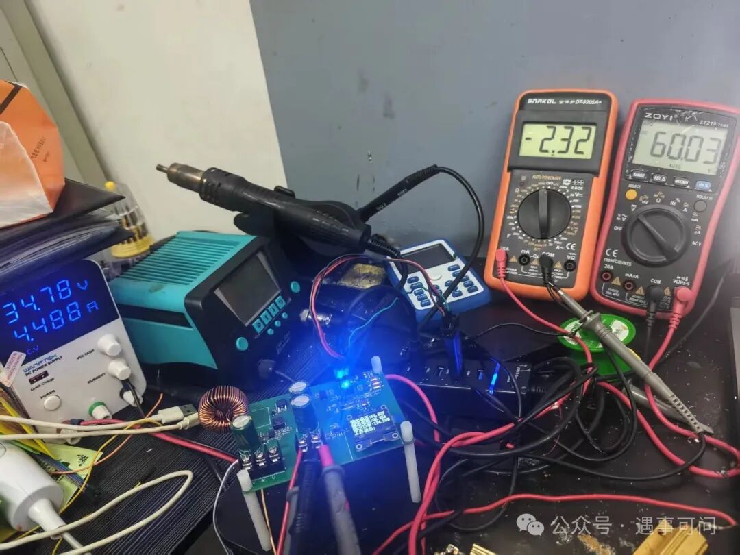
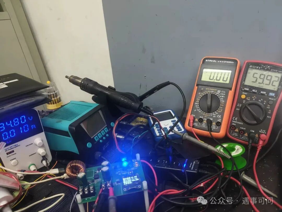
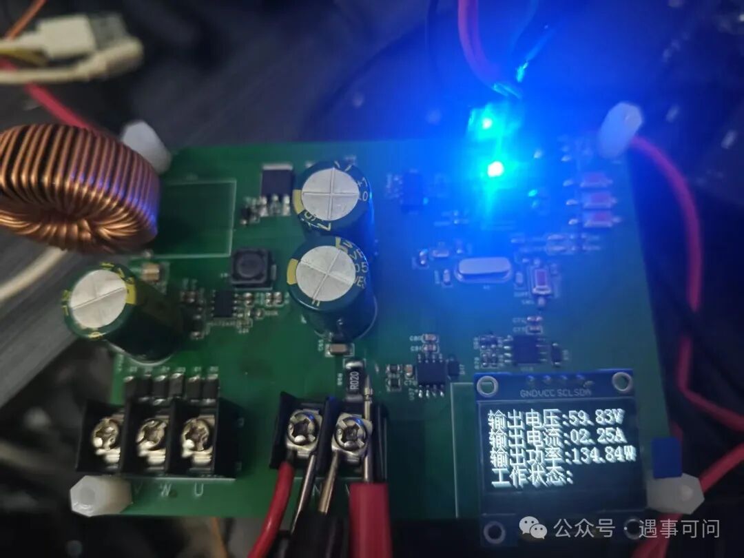 Input 35V, output 60V, calculated efficiency is 90%, which is not very high. The load adjustment rate is 0.18%. Areas for improvement include replacing the MOSFET with a higher performance one and increasing the output frequency of the microcontroller. The output capacitor’s capacity can be reduced; I used two 470uF capacitors in parallel. Since I used the LM358 operational amplifier, the larger the output voltage, the greater the voltage error collected. I have already compensated for the output voltage in the code, reducing the error range. To improve the error further, a high-precision operational amplifier can be used for voltage collection.6.2 Constant Current Test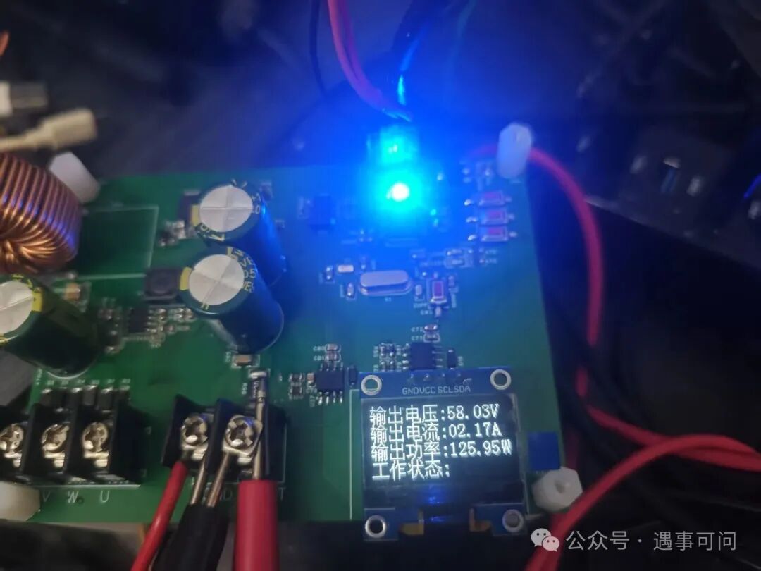
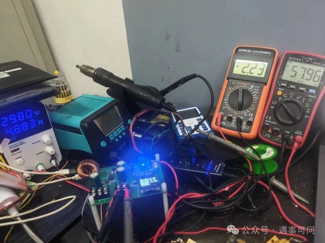 Input 30V, output set to 2.2A, actual error is 0.03A.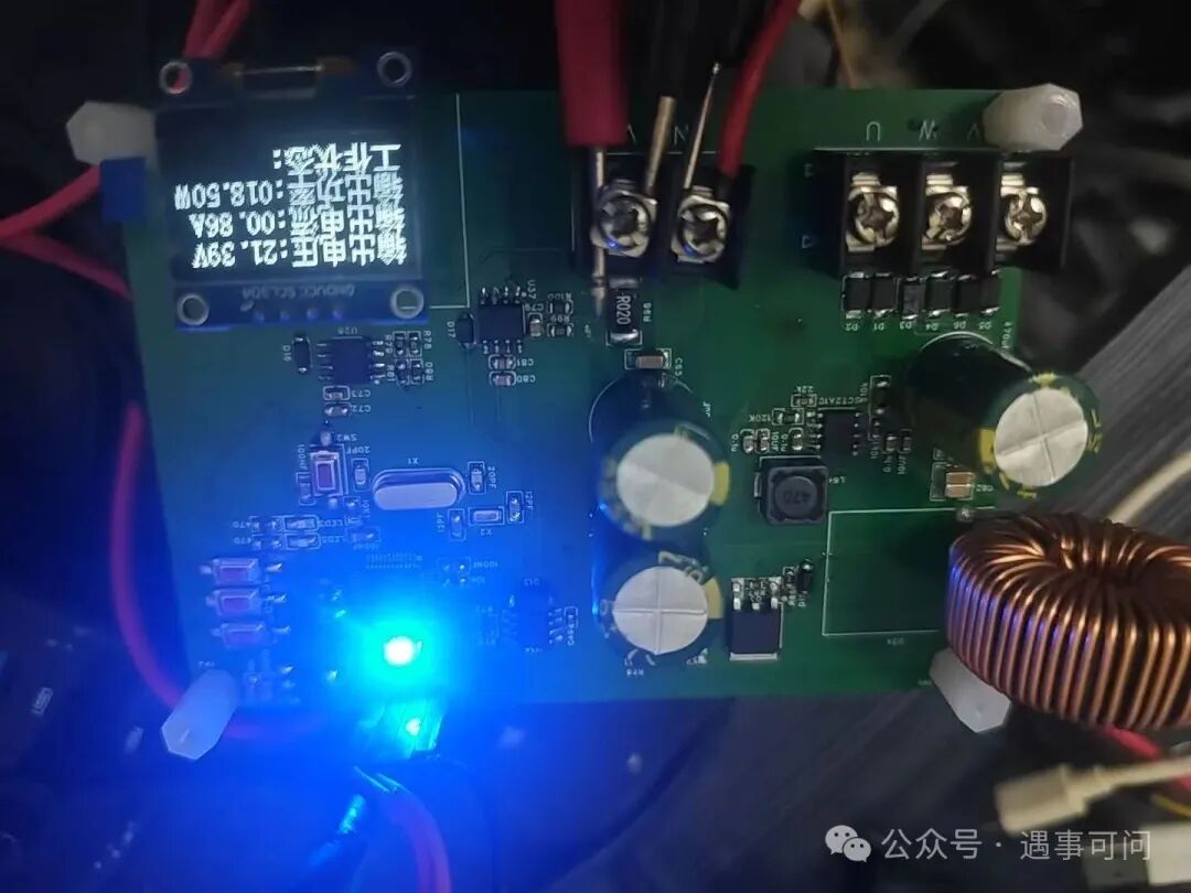
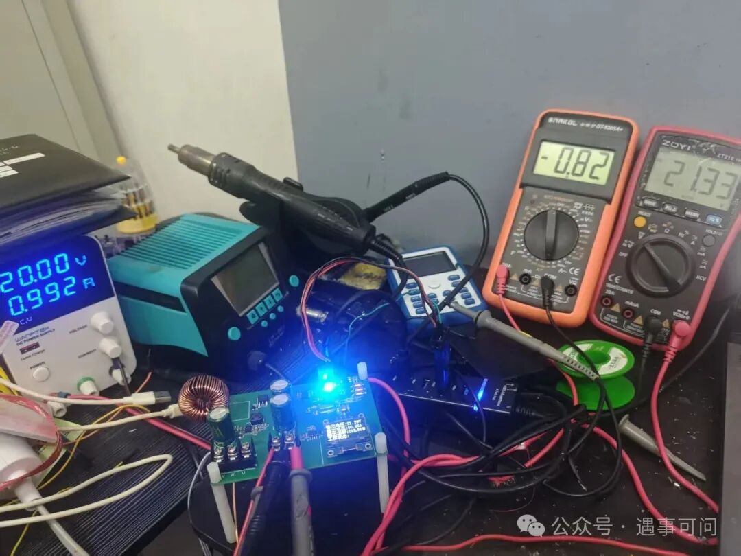 Input 20V, output set to 0.8A, output current is 0.82A, actual error is 0.02A.