Solder Bridging
An excess conductive pathway formed by solder between wires.
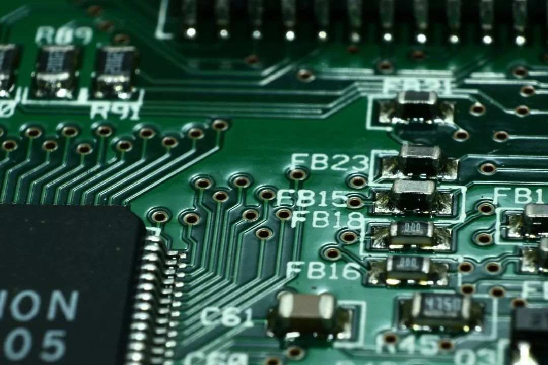
The bridging phenomenon is a type of soldering problem in PCBs, referring to the excessive solder that causes PCB pads to connect together. Unlike tombstone defects, bridging is not easily detected. However, it can cause fatal damage to the PCB.

Tombstone refers to a situation in PCBA processing where one end of a component does not touch the pad and stands up at an angle or stands upright while touching the pad.
Causes of Bridging
-
Excess solder on pads due to incorrect stencil size; -
Poor contact between stencil and bare board; -
Pads that are too large with insufficient solder mask; -
Incorrect placement of components or mismatch between component leads and pad sizes; -
Insufficient solder mask between pads.
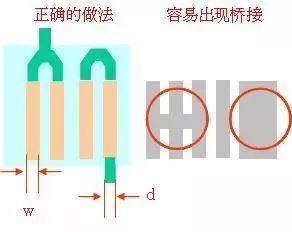
[Reminder] Engineers should pay attention to the situation where adjacent pads need to be connected during PCB layout: if adjacent pads need to be connected, first confirm the connection outside to prevent them from bridging together, and also pay attention to the width of the copper lines at this time.
(Content organized from the internet.)
Term 31

Want to expand and improve your hardware skills? Want to enhance your competitiveness in the workplace? Why not start by learning schematic design? Scan (recognize) the QR code below to learn Orcad schematic design practical course on “Tencent Classroom”: “4 Weeks to Learn Schematic Design through VR”.

▲ Scan to listen to the course “4 Weeks to Learn Schematic Design”