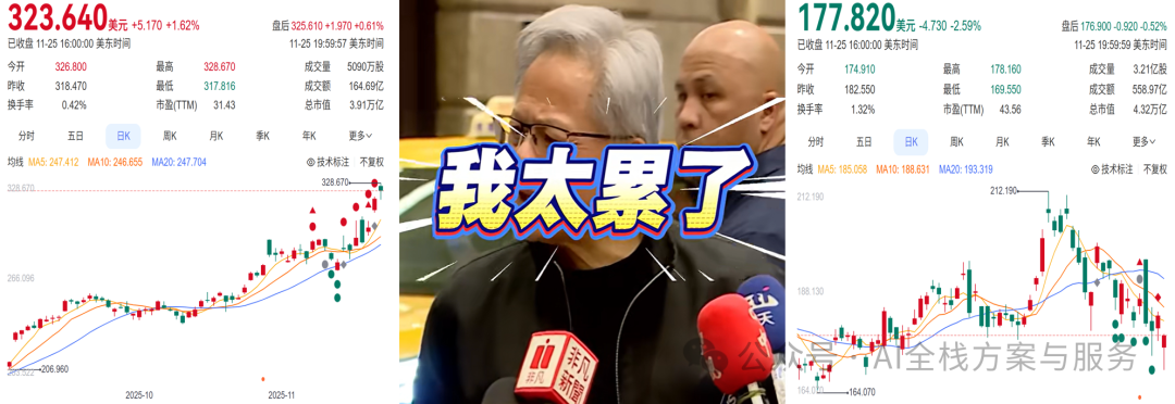
On the left is Google, representing specialized acceleration, and on the right is NVIDIA, representing general acceleration.
This does not constitute investment advice!!!
In today’s rapidly developing artificial intelligence technology, hardware infrastructure has become a key factor determining algorithm performance and application implementation.After the release of Gemini 3, the performance of models trained on Google’s latest TPU architecture has attracted widespread attention in the industry, with significant advantages in energy efficiency and large-scale training, posing a huge challenge to NVIDIA’s long-dominant GPGPU ecosystem.This competition between companies is, in fact, a philosophical clash between two different technological paths—general parallel computing and specialized optimization design. To understand the deeper significance of this transformation, we need to start from the essence of AI chip architecture and analyze the internal logic of technological evolution.
1.From Graphics Rendering to the AI Revolution: The Rise and Limitations of GPUs
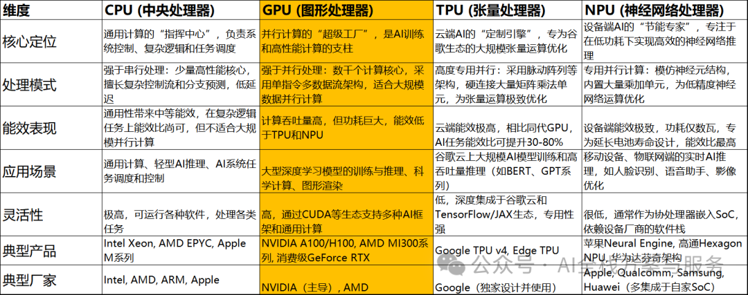
The glory of GPUs began with graphics processing.Early GPU architectures focused on solving parallel computing problems in graphics rendering, processing thousands of small computing cores simultaneously to handle pixels, vertices, and other graphical elements.When deep learning emerged in the mid-2000s, researchers keenly discovered that the matrix operations in neural network training bore a striking similarity to graphics rendering—both required handling highly parallel mathematical computations.
NVIDIA’s launch of the CUDA platform in2006 marked a turning point, transforming GPUs from graphics-specific chips into general parallel computing engines.CUDA architecture consists of computing arrays made up of thousands of streaming multiprocessors (SMs), each containing multiple CUDA cores capable of executing thousands of threads simultaneously. This “many-core” design demonstrated remarkable performance in processing convolutional neural networks (CNNs) and recurrent neural networks (RNNs), makingGPUs the standard for deep learning training..
However, the limitations of GPU architecture have gradually become apparent. Asa general parallel computing platform, GPUs must maintain complex control logic, branch prediction mechanisms, and support for diverse data types, which are essential components in general computing but become efficiency bottlenecks in pure AI computing.More critically, the memory architecture of GPUs is not optimized for tensor operations—frequent data transfers between global memory, shared memory, and registers lead to a significant “memory wall” problem, causing many computing units to remain idle while waiting for data.
2.Architectural Revolution:TPU from Systolic Arrays to Tensor Cores
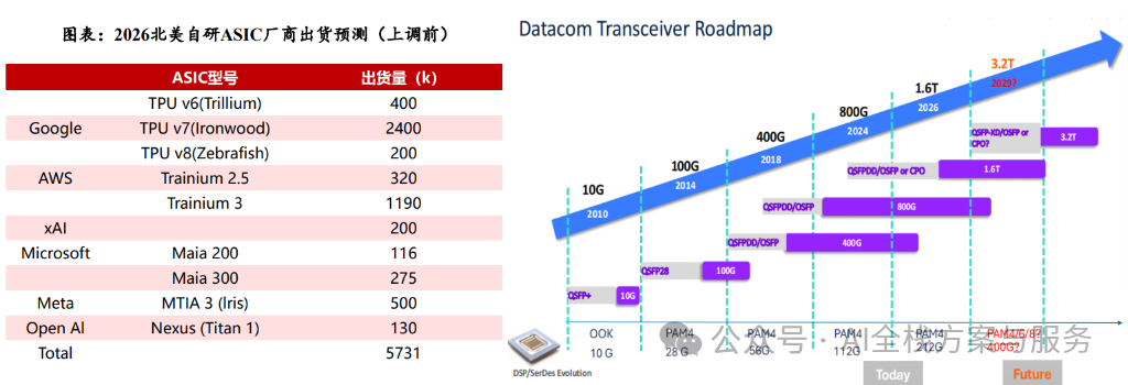
The origin of TPU can be traced back to Google in 2006. At that time, they were evaluating whether to use GPUs, FPGAs, or custom ASICs. Only a few applications required specialized hardware, and they judged that surplus CPU power from large data centers could meet these needs. However, this situation changed in 2013 when Google’s voice search function was running on neural networks, and internal predictions indicated that if this function developed, it would require far more computing power than before..
Thus, Google’s TPU represents a completely different design philosophy. As an ASIC (Application-Specific Integrated Circuit) specifically designed for machine learning,TPU discards the burdens of general computing at the architectural level, not needing to run general business applications, but it can efficiently handle the large matrix operations used in neural networks.
The core innovation of TPU lies in its “systolic array” architecture. This design originates from academic research in the 1970s but has been perfectly implemented in TPU. The systolic array consists of a grid of numerous multiply-accumulate units (MACs), with data “pulsing” through the array like blood in veins. When weight data flows in from one side and activation values flow in from the other side, they complete multiplication and addition operations in the MAC units at the intersection, and the results are passed along the diagonal direction. This designminimizes data movement, eliminating the need to access memory, allowing computing units to remain almost continuously active, achieving extremely high computational density.
For example, Google’s latest Ironwood TPU v7 has a theoretical peak performance of 4,614 TFLOPS, which is attributed not only to advancements in manufacturing processes but also to architectural optimization. TPU v7 introduces finer 8-bit precision support, significantly improving energy efficiency while ensuring model accuracy.
The performance of Google’s latest TPU has caused a stir not only due to its absolute performance metrics but also because it reveals the immense potential of specialized architectures in AI computing. Data shows that when training language models with hundreds of billions of parameters, TPU v7 can reduce training time by 40% compared to contemporary GPUs while lowering energy consumption by 60%. This gap translates to millions of dollars in cost differences in large-scale commercial applications.
More critically, TPU has advantages in scalability. When scaled to thousands of chips, TPU Pods exhibit nearly linear acceleration, while GPU clusters face diminishing returns due to communication overhead and load imbalance. This gives TPU a decisive advantage in training the largest models—at the forefront of current AI competition.
3.Energy Efficiency: The Decisive Advantage of Specialized Architectures
In the competition for AI chips, energy efficiency has become a more critical metric than absolute performance. As model sizes grow exponentially, training costs and energy consumption have become major bottlenecks constraining AI development. Google’s research data indicates that TPU improves energy efficiency by 30-80 times compared to contemporary GPUs when performing deep learning tasks. This gap is particularly significant in large-scale training scenarios.
The energy efficiency advantage stems from TPU’s precise grasp of the essence of computation. Over 80% of operations in deep learning are matrix multiplications, and TPU directly optimizes this core operation through dedicated hardware units, avoiding the large number of redundant operations that general computing units in GPUs perform when handling AI tasks. For instance, in the self-attention mechanism calculations of the Transformer model, TPU’s systolic array can decompose the multiplication operations of Q, K, and V matrices into forms most suitable for hardware execution, while GPUs need to map these operations to their general computing units through complex scheduling, leading to efficiency losses.
Additionally, TPU has been deeply optimized for the static characteristics of AI workloads. Unlike the variable scenes in graphics rendering, the computational graph of neural networks remains relatively fixed during training. TPU leverages this characteristic to complete the optimization and hardware mapping of the computational graph during the compilation phase, significantly reducing runtime scheduling overhead. In contrast, GPUs must retain sufficient flexibility to handle various possible computation patterns, and this generality inevitably leads to efficiency losses.
4.The Ecosystem Game: Software Stack and Development Experience
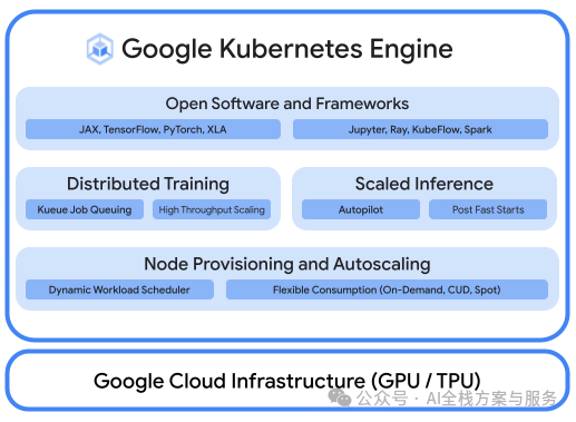
Hardware performance is only one aspect of competition; ecosystem development is equally crucial.NVIDIA has established a near-monopoly position with its CUDA ecosystem. CUDA not only provides a low-level programming interface but also builds a complete software stack, including optimization libraries like cuDNN and TensorRT, as well as deep integration with frameworks like PyTorch and TensorFlow. This ecological advantage makes GPUs the preferred choice for most AI developers.
However, Google is building an efficient software stack exclusive to TPU through the deep integration of the XLA compiler and TensorFlow. XLA compiles high-level framework operations into machine code optimized for TPU architecture, achieving global optimization of the computational graph. More importantly, the close integration of TPU with TensorFlow allows developers to leverage the full performance of TPU with minimal code modifications. For teams accustomed to TensorFlow, this seamless transition significantly lowers the barrier to adopting TPU..
A key turning point is TPU’s support for PyTorch. With the XLA backend, PyTorch models can now run efficiently on TPU, breaking down framework barriers and allowing a broader developer community to experience the advantages of TPU. As the PyTorch ecosystem expands to TPU, NVIDIA’s traditional advantages in software ecology are being challenged.
5.Essential Technical Differences: Data Flow vs. Control Flow
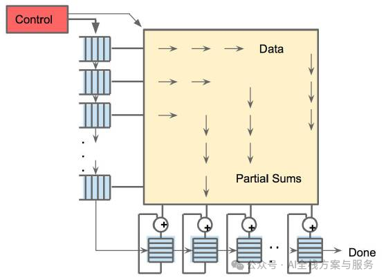
To truly understand the performance differences between TPU and GPU, one must delve into the architectural-level designs of data flow and control flow.
GPU is essentially a multi-threaded SIMT (Single Instruction, Multiple Thread) architecture. It groups similar computational tasks, allowing multiple threads to execute the same instruction simultaneously but on different data. This design is extremely efficient in graphics rendering but has inherent limitations in AI computing: when threads encounter conditional branches, they must undergo “thread divergence,” leading to some computing units being idle; moreover, the thread scheduling overhead of GPUs is particularly evident when handling small, irregular AI operations.
TPU, on the other hand, adopts a purer data flow architecture. In the systolic array, the activation of computing units is directly triggered by the arrival of data, eliminating the need for complex thread scheduling. This “data-driven” approach perfectly aligns with the strong data dependencies and simple control flows characteristic of neural networks. TPU v7 further introduces a smarter data prefetching mechanism that can predict computational needs and load data into the vicinity of computing units in advance, significantly reducing memory access latency.
In terms of memory hierarchy, TPU also demonstrates targeted optimizations. GPUs use a hierarchical memory design (registers, shared memory, global memory), requiring programmers to explicitly manage data movement; whereas TPU abstracts this complexity away through a unified virtual address space and automatic data flow management, allowing developers to focus on the model itself. This design is particularly effective in large-scale distributed training, as TPU Pods can seamlessly scale to thousands of chips without requiring developers to handle complex communication details.
6.Future Outlook: Heterogeneous Computing and Architectural Integration
Although TPU shows significant advantages in specific scenarios, the future of AI chips is not about the victory of a single architecture but rather moving towards more refined heterogeneous computing. Different architectures will play valuable roles in their respective strengths:
TPU will continue to dominate large-scale cloud training, especially within the Google Cloud ecosystem;
GPU will maintain its advantages in scenarios requiring flexibility, such as multimodal model training and the integration of scientific computing with AI;
Emerging architectures like optical computing and quantum-inspired AI chips may open new avenues in specific fields;
A noteworthy trend is architectural integration. NVIDIA is drawing on TPU’s design philosophy to enhance its GPUs’ specialized AI features; while Google is also incorporating more general computing capabilities into TPU to support a broader range of AI workloads. Huawei plans to add more general features and computing power on top of its NPU architecture. This mutual borrowing will drive the entire industry towards greater efficiency.
7.Conclusion: From Hardware Competition to a Shift in Computational Paradigms
The competition between Google’s TPU and NVIDIA’s GPU, on the surface, is a contest between two hardware architectures, but it fundamentally represents a shift in computational paradigms. The evolution from general computing to domain-specific architectures (DSA) reflects a transition in computational demands from “processing everything” to “optimizing key tasks.” In the AI-driven era, this shift is not only a technical choice but also a necessary requirement for efficiency and sustainability.
As model sizes continue to expand, energy efficiency will be a key factor determining whether AI technology can sustain its development. The specialized optimization route represented by TPU may become a decisive factor in the future AI infrastructure regarding energy efficiency. However, the ultimate victory of technology does not lie in the superiority of a single architecture but in the ability to build a complete ecosystem that adapts to diverse AI needs.
This deep game of chip architecture will ultimately push the entire industry beyond mere performance competition towards a more efficient and sustainable future of AI computing. For users, it is essential to understand the essential differences between various architectures and make the most suitable choices based on specific application scenarios.