Abstract: Aiming at the shortcomings of conventional DC power supplies, which have low output voltage accuracy and cumbersome adjustments, a high-precision NC adjustable linear DC power supply is designed. This power supply has an adjustable output voltage of 0-30 V and a maximum output current of 4 A. The accuracy of the output voltage is improved through a closed-loop negative feedback circuit consisting of output voltage/current sampling circuits, differential amplifier circuits, and voltage/current adjustment circuits, as well as a software-based bilinear interpolation error compensation method. The maximum output voltage and current can be adjusted using a rotary encoder and physical buttons, or set directly via a virtual keyboard created in the touch LCD module, making operation simple. Actual test results show that this power supply has high output voltage accuracy, with a load regulation rate of only 0.15% at 12 V output, and the parameter setting operation is straightforward, meeting the application needs for general teaching and scientific research.
A DC power supply is one of the commonly used instruments in the field of electronic technology, capable of providing stable DC output voltage when fluctuations occur in the grid voltage or load changes. Conventional DC power supplies consist of components such as a power transformer, rectification, filtering, and voltage regulation circuits, mostly employing a series feedback voltage regulation principle by adjusting the potentiometer in the output sampling branch to change the output voltage value. Due to the non-linear changes in the resistance of the potentiometer and the limited adjustment range, the output voltage accuracy of ordinary DC power supplies is not high. Over time, poor contact in the band switch used for coarse adjustment and the potentiometer used for fine adjustment can also significantly affect the output voltage, making adjustments cumbersome.
In response to the aforementioned shortcomings of conventional DC power supplies, a NC adjustable DC power supply is designed, with an adjustable output voltage of 0-30 V and a maximum output current of 4 A, high output voltage accuracy, strong stability, and easy parameter setting operations, which can also monitor and display the actual voltage/current output values in real-time.
1 System Design Scheme The overall design scheme of the system is shown in Figure 1, which mainly includes a rectification and filtering unit, output voltage/current sampling and adjustment circuits, a microprocessor unit, a display control unit, and commonly used voltage output units.
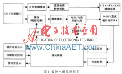
This power supply utilizes operational amplifiers to amplify the error between the output set value and the actual output value, adjusting the working point of the MOSFET through a closed-loop negative feedback circuit to achieve stable and controllable voltage/current output, featuring both constant voltage and constant current modes.
The system is equipped with two display control modes: one is the traditional physical button and knob parameter setting adjustment method to meet operational habits; the other is a touch control display method, where parameter settings are completed through virtual buttons, providing rich display information and flexible operation. Both display control modes work in coordination and include functions such as step switching, output enabling, and button locking. The voltage step values can be 1 V, 0.1 V, and 0.01 V, while the current step values can be 100 mA, 10 mA, and 1 mA. Additionally, to meet conventional voltage application needs in certain scenarios, four fixed voltage outputs of 3.3 V/3 A, 5 V/3 A, and ±12 V/1 A are realized using a switching power supply module and a DC power conversion circuit.
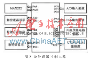
2 Main Hardware Circuit Design 2.1 Microprocessor Unit The microprocessor unit is the control core of the system, mainly responsible for input collection from mechanical buttons, knobs, and touch display units, as well as output display control. The specific control circuit is shown in Figure 2. In this design, the STM32F103VCT6 chip from ST, based on the ARM 32-bit Cortex-M3 core, is selected, with a maximum operating frequency of 72 MHz and a maximum speed of 90 MIPS. The chip integrates two 12-bit A/D converters and two 12-bit D/A converters, simplifying the peripheral circuit design and meeting the minimum output voltage/current resolution requirements.
2.2 Output Voltage/Current Sampling Circuit The output voltage/current sampling circuit is shown in Figure 3. The output voltage sampling is completed by a differential attenuation circuit composed of operational amplifiers, using OP07, which has a very low input offset voltage to ensure the accuracy of the power supply output. The two differential input terminals sample the output voltage in real-time and attenuate it proportionally. One path is low-pass filtered before connecting to the integrated A/D converter inside the microprocessor, while the other path connects to the voltage error amplification circuit. To ensure the accuracy of the attenuation coefficient, R28, R17, R31, and R15 are all high-precision, low-temperature drift resistors. When the power supply output voltage is adjusted within 0-30 V, the voltage sampling value changes linearly within 0-2.44 V.
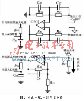
Output current sampling is completed by a non-inverting amplifier circuit composed of operational amplifiers. R47 is a 5 W high-power, low-temperature drift precision resistor with a resistance value of 0.05 Ω, achieving a linear conversion from 0-4 A current values to 0-0.2 V voltage values. The voltage signal across the sampling resistor is amplified, with one path low-pass filtered before connecting to the integrated A/D converter inside the microprocessor, while the other path connects to the current error amplification circuit.
2.3 Voltage/Current Error Amplification Circuit Design
When the power supply operates in constant voltage mode, the current feedback loop only serves to limit the current. When the actual output current is less than the set limit, the current error amplifier operates in the positive saturation zone, while the voltage error amplifier operates in the linear region. When the load changes cause a slight increase in the output voltage, the output of the voltage error amplification circuit reduces the gate-source voltage of the MOSFET, thus reducing its conduction degree and lowering the output voltage until the actual output voltage equals the set voltage. Conversely, when the load changes cause a slight decrease in the output voltage, the output of the voltage error amplification circuit increases the conduction degree of the MOSFET, raising the output voltage until it equals the set voltage.
This power supply operates in constant current mode, where the adjustment principle of the current error amplification circuit is similar.
2.4 Adjustment Tube Temperature Sampling Circuit In the system design, the adjustment tube temperature sampling circuit serves two main purposes: (1) Providing real-time temperature data for system overheat protection. When the temperature is below 35℃, the cooling fan is turned off. When the temperature is between 55℃ and 80℃, the fan is turned on. If the temperature exceeds 80℃, the power output is turned off; (2) Providing parameters for error compensation of the voltage output value: when the adjustment tube temperature or load current varies widely, the output voltage accuracy of the power supply will be affected. The system uses a two-dimensional linear interpolation algorithm for compensation to achieve high precision output, with the adjustment tube temperature being one of the important parameters in the algorithm.
This system employs the LM35 chip to achieve real-time sampling of the adjustment tube temperature. This chip features ease of use, high linearity, a wide temperature measurement range, and low self-heating, among many advantages. Additionally, this chip requires no debugging or calibration during use, has simple wiring, and low output impedance.
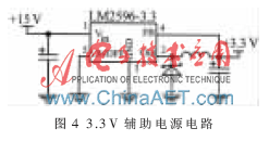
2.5 Auxiliary Power Supply Circuit To meet the conventional voltage application needs in certain scenarios, a switching power supply module is used to convert 220 V AC to ±15 V DC output, which is then processed through a DC power conversion circuit to achieve four fixed voltage outputs of 3.3 V/3 A, 5 V/3 A, and ±12 V/1 A. The 3.3 V and 5 V DC power supplies are realized using the LM2596 from National Semiconductor, which is a step-down voltage regulator integrated circuit capable of outputting a maximum of 3 A drive current, with excellent linearity and load regulation capability. The design selects LM2596-3.3 and LM2596-5.0 for the 3.3 V and 5 V power supplies, respectively, with simple peripheral circuit configurations, as shown in Figure 4. The ±12 V power supply adopts conventional 7812 and 7912 three-terminal voltage regulator circuit designs.
3 System Software Design
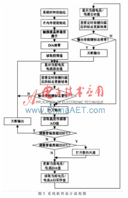
This system software adopts modular programming in C language, utilizing Keil MDK-ARM for compilation. The software design flow is shown in Figure 5. The software system mainly consists of the following modules: (1) Main function module: The main function initializes the system, reads the D/A calibration values at startup, and displays the initial voltage and current settings; it then starts scanning for button presses. If a button is pressed, it sets the output voltage through D/A and reads the adjustment tube temperature sampling value to determine whether to turn on the fan or perform overheat protection. (2) Button timing scanning function module: The system checks the control panel every 5 ms. If a new voltage/current setting value is input, it immediately updates the corresponding flag. (3) Digital tube display update function module: Whenever the real-time voltage or current signal changes, the microcontroller actively updates the display results of the digital tube. (4) Serial communication function module: The microcontroller communicates with the touch LCD screen through the serial port. Interrupts are used to receive touch information from the LCD screen, improving CPU real-time performance and work efficiency; polling wait mode is used to send voltage/current and step value display information to the LCD screen to ensure the completeness of each data frame. (5) D/A conversion function module: For ease of data processing, the program algorithm uses floating-point numbers in the ranges of 0.00-30.00 and 0.000-4.000 to represent the set voltage/current values. This function module linearly converts these representation ranges to the required 0-4095 range for the 12-bit D/A. (6) Voltage/current step adjustment function module: The voltage step values can be 1 V, 0.1 V, and 0.01 V, while the current step values can be 100 mA, 10 mA, and 1 mA. This function module implements addition and subtraction adjustments based on different step values.
4 Error Analysis and Compensation
When the power supply is operating normally, the maximum temperature of the adjustment tube under high current and heavy load conditions is around 60℃, while it fluctuates around normal temperature under low current and light load conditions. Ensuring the output voltage accuracy when the adjustment tube temperature or load current varies widely is one of the challenges in the design of this power supply. The output voltage accuracy is mainly determined by several factors: the precision and temperature drift of the operational amplifier’s peripheral resistors in the voltage sampling circuit; the offset voltage and temperature drift of the operational amplifier; the performance of the D/A converter and the temperature drift of the voltage reference source. In this design, high precision, low temperature drift, and well-performing key components are selected from the hardware side, and software-based two-dimensional linear interpolation compensation for the D/A output values is performed to ensure precise output voltage even when the adjustment tube temperature or load current varies widely.
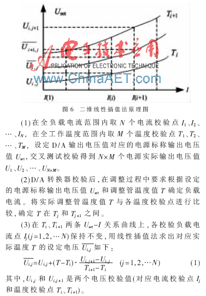
Based on the above analysis, to ensure the accuracy of the output voltage across the full load current range and the full operating temperature range, the D/A value sent to the voltage error amplification circuit needs to be compensated based on the load current I and environmental temperature T. The two-dimensional linear interpolation algorithm adopted by the system is illustrated in Figure 6.
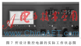
5 Experimental Results Based on the above design scheme, a NC power supply has been fabricated, and its actual working state is shown in Figure 7.
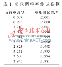
One of the main parameters of the designed power supply, the load regulation rate, was tested. The experimental setup was as follows: The load applied to the power supply output terminal was a 150 W micro in-car inverter powered by 12 V DC (with an effective output voltage of 220 V at a frequency of 50 Hz). This inverter was connected to a 50 W adjustable incandescent lamp to achieve adjustable load. The NC power supply output voltage was set to 12.00 V, with a maximum output current of 4.000 A, and the brightness of the incandescent lamp was adjusted using the adjustment knob, measuring the output voltage under different load conditions using a 6.5-digit Agilent 34401A multimeter.
The test data is shown in Table 1, from which the load regulation rate of the power supply at 12 V output is calculated to be 0.15%.
This article designs and manufactures a high-precision NC power supply, which has an adjustable output voltage of 0-30 V, a maximum output current of 4 A, a minimum voltage step value of 0.01 V, a minimum current step value of 1 mA, and a load regulation rate of less than 0.2%. The power supply is equipped with two display control schemes, allowing control via physical buttons and knobs, as well as touch control of output voltage/current values through a touch LCD screen. A notable feature of the touch LCD screen operation scheme is the addition of direct keyboard setting functionality, making operation simpler. Additionally, the power supply is equipped with four common fixed voltage outputs and has a comprehensive protection function, meeting the requirements for general experiments and teaching activities. Furthermore, through system software programming, the power supply can achieve extended functions such as customized output voltage waveforms.
References
[1] Zhu Guixian. Design of NC Voltage Regulator Based on Microcontroller [J]. Automation and Instrumentation, 2011(6):50-53.[2] Liu Chuxiang, Du Yong, You Shuangfeng. Design of NC DC Voltage Regulator Based on Microcontroller [J]. Journal of Xinjiang Normal University (Natural Science Edition), 2007, 26(1):50-52.[3] Amo Electronics Forum. Electronic Technology Exchange [EB/OL]. (2013-03-22) [2013-05-01]. http//www.amobbs.com.[4] Lin Yingquan, Li Hongwen. Design of Theodolite Switching Power Supply Monitoring Module [J]. Instrument Technology and Sensors, 2010(11):15-17.[5] Wu Hongyi, Chen Bo, Yu Zhouping. Design of DAC Nonlinear Compensation System Based on Temperature Sensor [J]. Sensors and Microsystems, 2011, 30(9):82-84.