Chip Manufacturing
In semiconductor manufacturing, batch processing and single wafer processing are essentially a dynamic balance of process precision, production efficiency, and cost control.
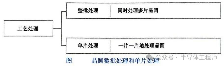
Batch processing achieves high throughput by processing multiple wafers simultaneously, making it suitable for mature processes with relatively relaxed uniformity requirements, such as thermal oxidation, chemical vapor deposition (CVD), and some wet cleaning processes. Its advantages include high production capacity per unit time and small equipment footprint, but the difficulty of controlling uniformity between and within wafers increases as design standards become stricter, especially in scenarios involving large diameter wafers over 300mm, where edge effects and chamber environment fluctuations can easily lead to pattern accuracy deviations.
Single wafer processing, on the other hand, ensures high consistency within and between wafers through precise processing, becoming the core choice for advanced processes. As chip feature sizes approach physical limits, the ability of single wafer processing to guarantee circuit pattern uniformity becomes increasingly critical— for example, in logic processes below 3nm, the combination of single wafer exposure and atomic layer deposition (ALD) processes can achieve sub-nanometer film thickness control, avoiding micro-loading effects caused by chamber temperature gradients or uneven gas distribution in batch processing. Furthermore, with the trend of wafer diameters expanding to 450mm, single wafer processing can more easily adapt to the uniformity requirements of large substrates by independently controlling the process parameters of each wafer, reducing pattern distortion caused by wafer bending or thermal stress.
However, the capacity bottleneck of single wafer processing always exists. To balance precision and efficiency, the industry is exploring hybrid processing strategies and intelligent scheduling systems. For instance, in deposition processes, batch CVD is used for basic film growth, while single wafer ALD is used for high-precision deposition of critical layers; in lithography processes, single wafer exposure machines combined with batch coating and developing equipment achieve a synergy of high-precision patterning at the front end and efficient processing at the back end. In recent years, AI-driven process optimization platforms have improved the production efficiency of single wafer processing by over 15% while reducing the defect rate by 30% through real-time monitoring of wafer status and dynamic adjustment of equipment parameters.
In the latest developments, single wafer processing is deeply integrated with 3D integration technology. For example, in the manufacturing of 3D NAND flash memory, single wafer etching and deposition processes can precisely control the alignment accuracy between stacked layers, supporting mass production of structures with over 200 layers; in the advanced packaging field, the combination of single wafer processing and hybrid bonding technology has achieved sub-micron interconnections between chips, driving performance leaps in system-in-package (SiP). Meanwhile, batch processing continues to play a valuable role in mature processes, such as batch diffusion furnaces in power device production, which optimize tube temperature distribution and gas flow to maintain uniformity while ensuring cost advantages.
In summary, the choice between batch and single wafer processing is not an either-or decision, but a comprehensive decision based on process stage, design requirements, and cost-effectiveness.
With the penetration of AI, the Internet of Things, and new material technologies, future semiconductor manufacturing will increasingly rely on intelligent process control systems to achieve dynamic optimization between batch and single wafer processing, continuously promoting the triangular balance of precision, efficiency, and cost, supporting the semiconductor industry towards finer and higher performance directions.
Source from Learning Those Things, Author Xiao Chen Po Po

Zhao Gong
13488683602
Submission/Promotion/Group Joining/ Reprint