Fundamentals of Buried Power Distribution Network (BSPDN)
In addition to Gate-All-Around (GAA) transistors, BSPDN is another key innovation in next-generation logic process technology. In all current digital logic process technologies, transistors are first fabricated on the wafer, followed by the creation of dozens of metal layers that power the transistors and transmit signals between them and the external world.
As circuits scale down, both transistors and interconnects must shrink. In the past, this was almost an afterthought, but today, scaling interconnects is more challenging than scaling transistors. For example, most extreme ultraviolet lithography (EUV) is actually used for interconnects (contact points, vias, and metal layers) rather than the transistor layers themselves. As the number of transistors on a chip increases, the number of interconnects also rises, driving a steady increase in the number of required interconnect layers. More layers mean higher manufacturing costs, difficulties in wiring design, and performance degradation due to longer signal paths.
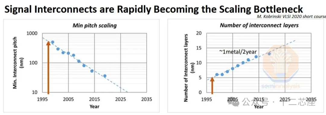
Source: Intel IEDM 2023
However, this does not mean that the industry has stopped progressing. Material innovations, design technology co-optimization (DTCO), and extreme ultraviolet lithography have driven the scaling of interconnects to current process nodes. However, as this pattern becomes increasingly expensive and limits the potential for further miniaturization, the calculations for implementing BSPDN begin to make sense. This is not a new idea; it is simply the right time for it. Innovations in interconnects are also overdue, as it has been nearly 30 years since the last evolution from aluminum to copper in 1997.
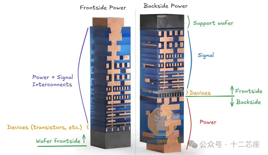
Source: Intel, SemiAnalysis
The core idea of BSPDN is to move the power distribution lines to the back of the wafer. This frees up space for signal wiring (retained on the front), while power is relocated to the back. Architecturally, this means that standard cells with a height of less than 6T (tracks) become more feasible. 6T refers to the height of standard cells, which are the basic building blocks of digital logic, such as NAND gates, and the height of these cells is typically measured in multiples of T, where T is the number of metal 2 layers (“tracks”) that the cell spans. Smaller cells are better: smaller cells can increase density without shrinking underlying features such as fins, gates, and metal interconnects. Shrinking more features is expensive as it requires better lithography techniques.
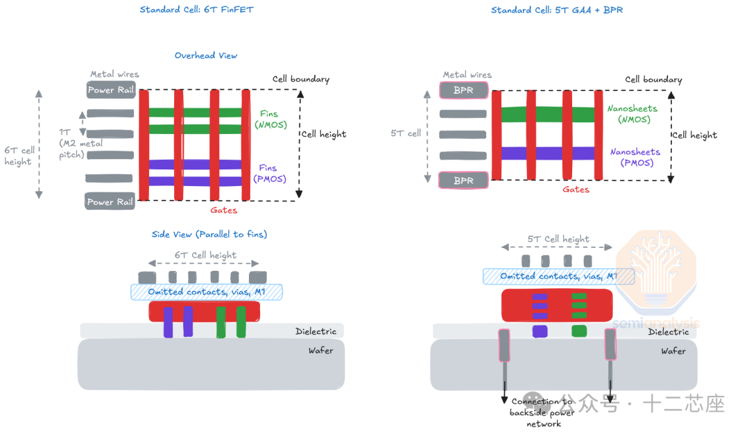
Standard cell scaling finFET vs. GAA + Buried Power Rail. Source: SemiAnalysis
From above, the top and bottom of the standard cell are constrained by wide metal tracks in the M2 metal layer. These tracks provide power and reference voltage to the cell and connect to other power distribution networks in higher metal layers. These tracks are part of the total 6T height of a typical front-only cell—moving them to the back means the cell can shrink to 5T or smaller.
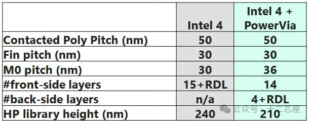
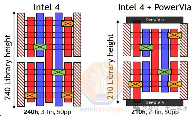
The architectural advantages of BSPDN: Increasing power vias can increase density through shorter cells while reducing costs by relaxing M0 spacing. Source: Intel
BSPDN improves power distribution in two ways. First, the interconnect length that powers the transistors is significantly shortened. Front-only power must traverse more than 15 layers of metal at the 3nm node, while back power may include fewer than 5 layers and uses thicker (lower resistance) wires. Therefore, power loss due to wire resistance can be reduced by about an order of magnitude.
Secondly, BSPDN reduces the need for aggressive interconnect scaling. The resistance of copper wires increases exponentially in the range of diameters less than 100nm. Today, the line widths of cutting-edge technologies are far below 20nm, and resistance becomes a critical issue. This is undesirable because high line resistance wastes power and generates excessive heat in the chip. This is not a permanent solution—scaling will continue, and alternatives to copper will be needed—but BSPDN provides relief.
Overall, compared to similar front-only processes, BSPDN can reduce power consumption by about 15-20% in high-performance designs.
There are currently three different methods of back power being explored and/or implemented: Buried Power Rail, Power Via, and Direct Backside Contacts.
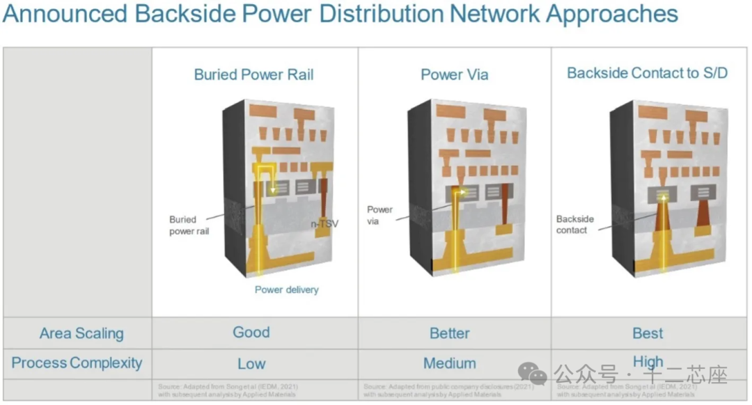
Source: Applied Materials
Buried Power Rail (BPR)
Buried Power Rail (BPR) is the simplest implementation of back power. Early research used this scheme, and subsequent architectures have expanded upon it. It involves moving the power rail from its usual position above the transistors in the M2 metal layer to an independent level below the transistors. This allows the architecture to shrink, as the wide power rail is replaced by a thin and tall rail that is closely placed beneath the transistors. However, the buried power rail still connects to the transistors through the front metal layers and connects to the back power distribution network via through-silicon vias (TSVs). This means the overall cell height can be reduced by about 1T, approximately 15%.
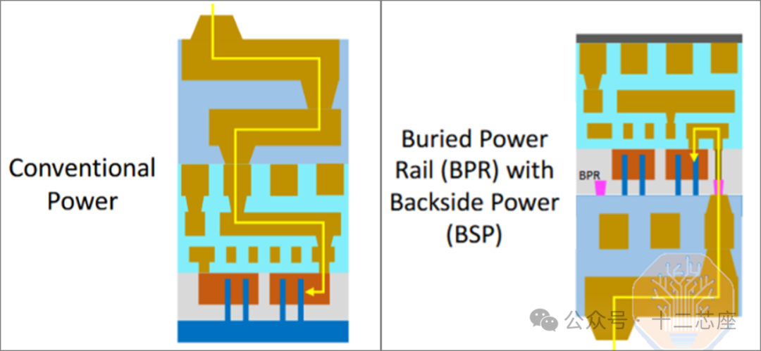
Comparison of traditional and BPR: Manufacturing buried power rail below the transistors on the wafer front, then connecting to the back power network. Source: Intel
Building a BPR is relatively straightforward, but there is a major risk: the use of metal in the front-end process. Traditionally, metals are limited to the middle-of-line (MOL) and back-end-of-line (BEOL) processes, used after the transistors are fabricated. This is to avoid contaminating semiconductor devices with conductive metals. Wafer fabs are very strict about this—many fabs have tools dedicated to front-end processes that are prohibited from being used on any wafers with metal layers. Fabs must break this rule to construct buried power rails, as BPRs must be completed before transistor integration. In practice, no one is willing to break this rule, and BPRs seem unlikely to be adopted by any high-volume manufacturing (HVM) processes.
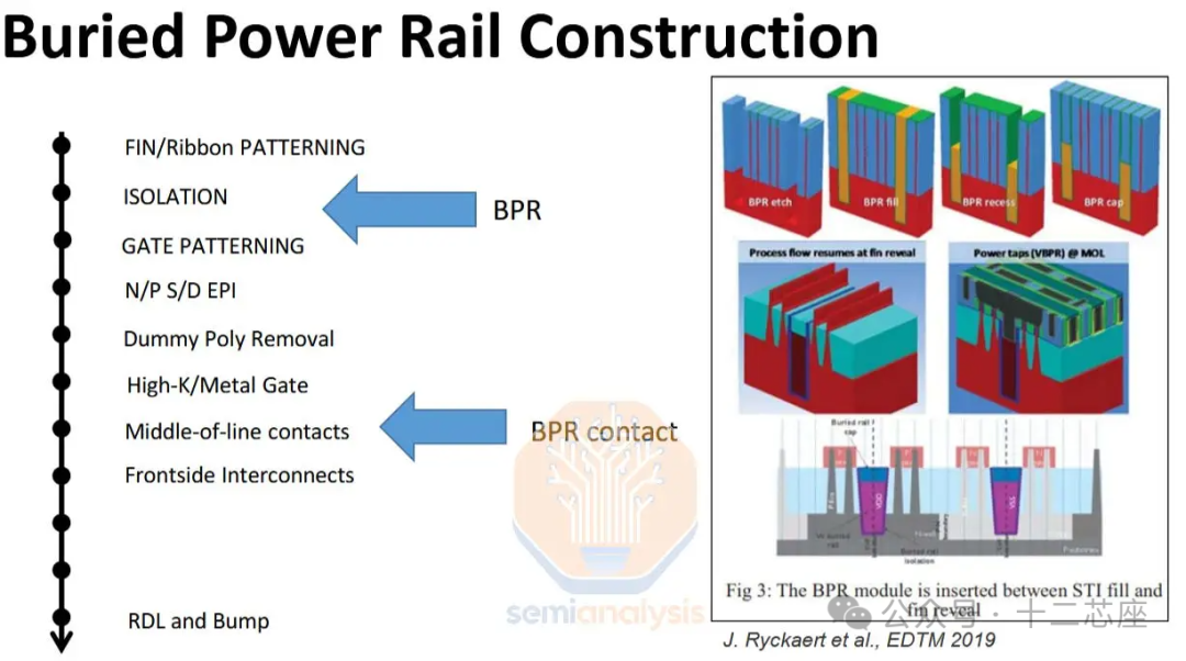
Buried Power Rail requires the use of metal in front-end processing steps. Source: Intel
Aligning the initial backside features connected to the buried rail is another challenge. The bonding that supports the wafer introduces distortions that need to be corrected, making post-bonding lithography more difficult. ASML and other companies have made significant progress in this area, and the post-bonding alignment capability is sufficient to meet BPR schemes—but for more complex options like direct backside contacts, it is already close to the limits of specifications.
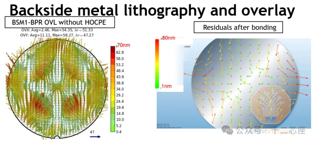
Source: imec
PowerVia
PowerVia is Intel’s back power solution. It improves BPR in two main ways:
Power rails are moved to the back of the wafer: avoiding the contamination risk of BPR.
Better cell scaling: as power wiring is eliminated from the front of the wafer.
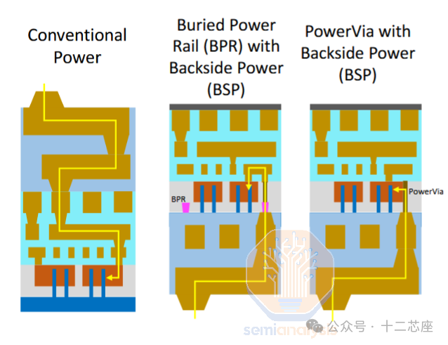
PowerVia connects to the sides of the transistor contact points, avoiding any power wiring on the front. Source: Intel
PowerVia is a clever evolution of the BPR concept. In the front-end processing, PowerVia completely skips the power rail. This not only avoids the contamination risk of depositing metal before the transistors but also eliminates an expensive alignment-critical process step (aligning the BPR to the transistor channel). At gigawatt wafer fab scales, the cost of such a critical layer can reach hundreds of millions of dollars.
The only additional step compared to traditional front-only schemes is the construction of the tall and thin PowerVia just after the transistor contact points. This via extends deep into the wafer substrate. After completing the front, the wafer is flipped, bonded, and thinned. Because the vias extend into the back of the wafer, they can be exposed during thinning without damaging the transistors. This clever “self-alignment” approach greatly simplifies the back patterning that must align with PowerVia (in this context, “self-alignment” actually means that alignment requirements are greatly relaxed, resulting in lower costs and higher yields).
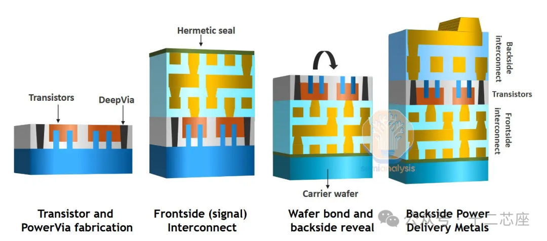
Source: Intel
This method also has scaling advantages. BPR connects to the transistors through vias above the transistor contact points, through the front metal layers, and then through another via to reach the BPR itself. These low metal layers are one of the key scaling limiting factors, as they require some minimum features and very crowded wiring—by wiring power through them, BPR does little to alleviate these issues. PowerVia helps here. Wiring directly from the transistor contact points down to the BSPDN means that there is truly no power wiring through the critical front metal layers. This means that the spacing of these layers can be relaxed (reducing costs), scaling can be more aggressive, and signal lines can replace the relocated power lines, or a combination of all three.
However, there is still room for standard cell scaling. Although PowerVia is thinner than BPR, it still contributes to the total height of the cell.

Direct Backside Contacts (DBC)
Direct Backside Contacts (DBC or BSC, i.e., backside contacts) provide a way to eliminate the contribution of power to the height of standard cells. In other words, they achieve the greatest scaling advantage of any back power scheme. The idea is a natural extension of BPR and PowerVia—rather than wiring power from the top or side of the contact points, it is wired from the bottom.
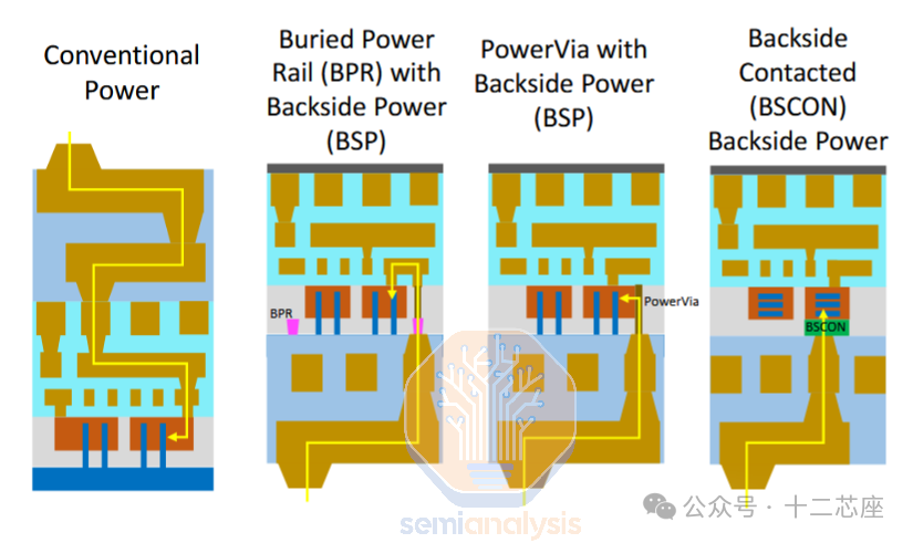
Source: Intel
Although the idea is simple, it turns out that backside contacts are the riskiest and most rewarding option for BSPDN. Manufacturing them is not easy. The main driver is the spacing, which is the tightness with which the contact points must align with other features. For BPR and PowerVia, the spacing to features connected to the back is roughly the same as the height of the cell, which for modern cutting-edge processes is about 150-250nm. The alignment accuracy required for post-bonding lithography to pattern the first layer of backside power is greater than 10nm. This level of alignment accuracy and spacing greater than 150nm can be easily achieved with cheaper deep ultraviolet (DUV) scanners.
For direct backside contacts, the requirements are much more difficult. The contact points for power wiring form beneath the source and drain. The distance from source to drain is roughly equivalent to the contact poly-silicon pitch (CPP), which is the distance from gate to gate. The CPP for modern processes is well-known, providing us with a rough requirement for backside contact spacing—about 50nm. This far exceeds the resolution of a single ArF immersion exposure, requiring more expensive multi-patterning schemes or extreme ultraviolet (EUV) lithography. Alignment accuracy also becomes a challenge, as specifications require less than 5nm. Typically, this is not an issue for high-end scanners, but due to wafer bonding locking in high-order distortions, it becomes extremely difficult here.
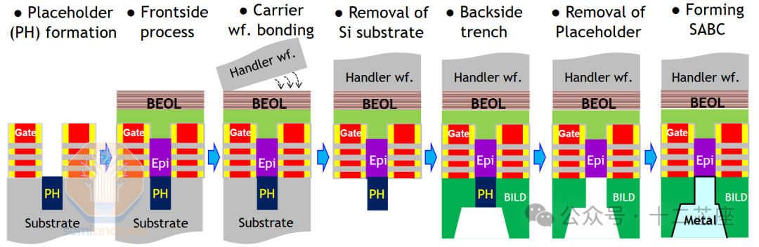
Self-aligned backside contact integration scheme using a non-conductive placeholder. Source: IBM + Samsung
Another challenge is the use of metal in the front-end process, but modern backside contact schemes have a clever workaround here. Like BPR, they require an additional feature to be fabricated before the transistors. However, the contact points are initially filled with non-conductive placeholder material instead of metal. Once the placeholder is revealed during thinning (like PowerVia, these features are self-aligned), they can be etched away and replaced with metal. This trick does not work well for BPR, as they are high aspect ratio, making it difficult to cleanly etch away the placeholder material.
Despite the challenges in manufacturing, the benefits of backside contacts are enormous: theoretically, a front-only 6T cell can shrink by about 25%, reaching 4.5T or even 4T. In practice, rather than shrinking the cell, it is better to wire signal lines in the position of the relocated power rails. This significantly improves wiring and still achieves density increases at the chip level. Line resistance is significantly reduced, power consumption is saved by about 15%. Clock frequencies can be increased by over 5%. Reliability improves as both front and back lines can be larger, reducing the risk of electromigration and allowing for faster switching or higher currents. A study published this year by IMEC, Google, and Cadence at VLSI found that high-power (HP) libraries achieved the greatest benefits, which are typically used for high-performance computing (HPC) applications such as AI accelerators.
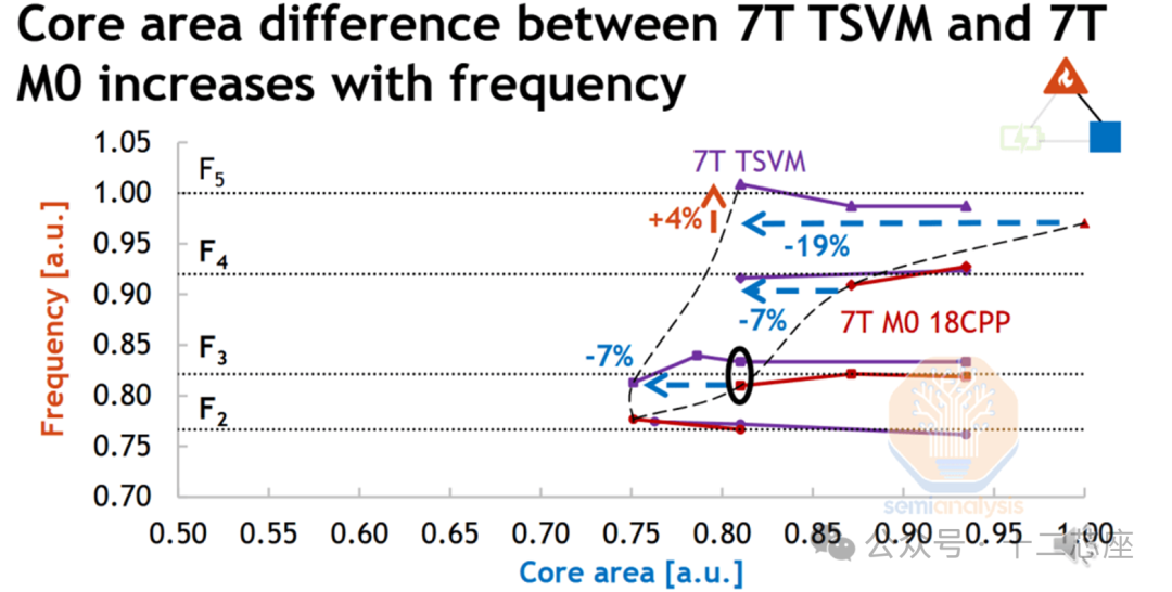
It is important to note that these benefits do not come without cost. The total layer count may increase by up to 20%. Wafer thinning, while not affecting active components like transistors, may degrade the performance of passive devices (like diodes) that rely on thick silicon—solutions need to be found. All backside processes must be compatible with front-end devices: that is, they cannot require high temperatures that would damage the transistors.
In the future, the back will not only be limited to power and global clocks. Signals and backend devices (such as capacitors, Intel has already demonstrated MIM capacitors in the back redistribution layer) are also likely to move. This will be important for stacked transistors (CFETs), as the signals from the underlying devices must be routed through the back wiring to achieve full scaling advantages. The 1.4nm node and beyond should start to include greater complexity on the back.
Disclaimer:The author respects intellectual property, and some images and content are sourced from the public network, with copyright belonging to the original publishing organization. If there is any infringement, please contact for timely removal.
Reference:
1.TSMC, Intel, Samsung, IBM, Rapidus, SemiAnalysis
2.https://semianalysis.com