The journey of a PCB from copper board to circuit is like a precision trip. Let’s take a look at the journey of a PCB’s birth.
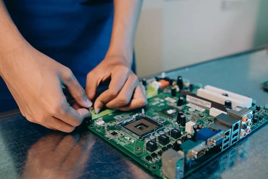
Step 1: Design Transfer – Creating the “Construction Blueprint”Convert the engineer’s design files into a universal format that all devices can understand, similar to transforming architectural blueprints into construction drawings that workers can comprehend.Check whether the design meets the factory’s process capabilities to avoid the risk of “shoddy engineering”. Step 2: Inner Layer Etching – Precisely “Carving Copper Wires”Apply a photosensitive film: Cover the copper-clad board with a special “fresh-keeping film” – the photosensitive film.Exposure and development: Use a “light carving” method to accurately replicate the circuit pattern onto the photosensitive film; the exposed areas will solidify to form a protective layer.Etching and cleaning: Use a chemical solution to “shower” the board, removing the unexposed film and etching away the unnecessary copper foil, revealing the circuit pattern, and finally peeling off the solidified protective film.Step 3: Layer Lamination – Creating a “Thousand-Layer Pastry”Stack the completed inner layers, prepreg (pre-impregnated material), and copper foil together like making a thousand-layer pastry.Send it into a vacuum hot press, where it is fused into a solid whole under high temperature and pressure.Step 4: Drilling Through Holes – Creating “Connection Tunnels”Use a high-precision drilling machine to create numerous small holes on the board; these holes will later connect the circuits of different layers.Copper plating the hole walls: Use a chemical method to “plate” a thin layer of copper on the insulated walls of the holes, making them conductive and truly creating “tunnels” between the layers.Step 5: Outer Layer Reinforcement – Thickening the “Copper Wire Armor”Transfer the circuit pattern of the outer layer onto the board.Thicken the copper layers on the circuits and hole walls through electroplating, enabling them to carry larger currents, akin to dressing the circuits in sturdy “armor”. Step 6: Solder Mask Application – Coating with “Insulating Green Paint”Apply green solder mask ink (the green layer you see) on the surface of the board, exposing the pads and holes that need to be soldered through exposure and development.This layer of “green paint” prevents short circuits during soldering and protects the circuits from oxidation and damage.Step 7: Surface Treatment – Protecting the “Soldering Gold Fingers”Perform surface treatment on the exposed pads, such as tin spraying or gold immersion.The purpose is to prevent oxidation of the pads and ensure good soldering performance in the future.Step 8: Testing and Shaping – Final “Health Check” Before ReleaseElectrical testing: Power on and check 100% of the board for open circuits, short circuits, and other functional issues.Shaping: Use CNC machines or molds to cut the entire board into the required shapes and sizes for the customer.Appearance inspection: Conduct final checks on the board’s appearance with both manual and machine assistance; once qualified, it can be packaged and shipped.
Scan the QR code to register for consultation
Get a detailed outline of the catalog