On February 6, 1959, a four-page application containing images and five pages of text was officially submitted to the United States Patent Office.
This was Texas Instruments’ (TI) patent application for the concept of monolithic integration, which is the first patent for what we now know as the ubiquitous Integrated Circuit (IC).
As the inventor, Jack Kilby had an epiphany six months earlier, conceptualizing the prototype of the integrated circuit, and five months prior, successfully demonstrating the first integrated circuit.
However, he did not have time to solve the interconnection problem..
The idea of monolithic integration includes two revolutionary new concepts: integration and interconnection.
What is integration?
All components of the circuit can be made from the same material (silicon), allowing the entire circuit to be integrated onto a single chip; this is integration.
What is interconnection?
Once all parts of the circuit are manufactured on a single chip, the connections between different parts—wires—can be printed onto the chip as part of the production process; this is interconnection.
Thus, the enormous costs and reliability risks associated with manually connecting numerous components would be eliminated.
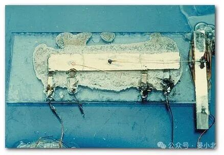
Kilby conceived the idea of integration but could not timely address the interconnection issue. The first integrated circuit chip he demonstrated was connected by extremely thin gold wires to discrete components,
and this chip looked like a gold spider web, with the flying wires making it unproducible.
By January 1959, Kilby had a vague idea that he could place a layer of silicon dioxide on top of the chip and print fine conductive metal lines on the silicon dioxide to connect different parts of the circuit.
However, prior to this, Fairchild’s Joan Horn had already conceived this idea and created a device in March 1959,
which is precisely what we now commonly refer to as a planar transistor.
Two thousand kilometers away in Texas, Kilby was unaware of this, but he had no time to ponder the interconnection issue.
At the end of January, a rumor quickly spread within TI—someone at RCA (Radio Corporation of America) had invented the integrated circuit and was preparing to file a patent.
The company had to act quickly, hiring lawyers to complete the patent text within a week,
which was named “Miniaturized Electronic Circuits” and was in its early form.
However, the application document had to include images, and the only available image was a crude demonstration chip from months earlier,
with the spider web-like gold wires suspended above the components. Kilby knew that this was the biggest flaw of the patent.
Later engineers often laughed at this image—it was called the “flying wire picture” because it looked nothing like the integrated circuits that would later be mass-produced.
To seize the initiative, TI had to use the flying wire picture,
Kilby and others tried to remedy the text, adding a paragraph to the application that explained Kilby’s vague idea,
“When making electrical connections, do not use gold wires,”“connections can be provided in other ways. For example… silicon dioxide can be evaporated onto the semiconductor circuit wafer. … Then, materials such as gold can be laid down on the oxide to make the necessary electrical connections.”
After completing the final additions, this four-page application with images and five pages of text was submitted to the patent office on February 6, 1959.
TI followed the standard application process, which took a long time.
Significant progress occurred two years after the application was submitted—on April 26, 1961, Kilby received a call from a lawyer in Washington,
informing him that the first integrated circuit patent in history had been granted.
However, it was not granted to TI or Jack Kilby.
By the 1950s, circuit manufacturing had nearly a century of history, but it followed the same method—purchasing discrete components such as resistors and capacitors separately and connecting them with wires.
The invention of the transistor could greatly enhance circuit efficiency, but it did not change the manufacturing method of circuits formed by interconnecting discrete components,
which was precisely the “digital tyranny” problem the industry faced in the 1950s.
In 1957, led by Noyce and Moore, the famous “traitorous eight” founded Fairchild Semiconductor,
and as the R&D director, Noyce was responsible for identifying key technical issues.
This was not too difficult, as the industry had been stalled for years in front of the “digital tyranny” wall, and frontier workers all knew this was a problem that needed to be solved.
Noyce later said he should have thought of the concept of monolithic integration earlier,
“What we were doing at the time was manufacturing all these transistor arrays on a single wafer, cutting them into small pieces, and then hiring thousands of women to pick them up with tweezers, trying to connect them together.”
“This was stupid, expensive, unreliable, and greatly limited the complexity of circuits you could build. The answer to the problem was, of course, not to cut them apart in the first place, but at that time, no one realized this.”
Noyce was trapped in a fixed mindset, trying to make circuit components smaller and more uniform, which was the wrong path, and he failed to come up with anything valuable.
Unable to break out of the fixed mindset, Noyce turned his attention to another technical problem—Fairchild’s then flagship product, silicon-based double-diffused transistors, were easily contaminated.
Upon dissection, it was found that metal shavings from the inner wall of the metal casing fell onto the PN junction, causing short circuits.
From a production perspective, it was difficult to solve this problem.
Fortunately, one of the “traitorous eight,” Joan Horn, solved this problem,
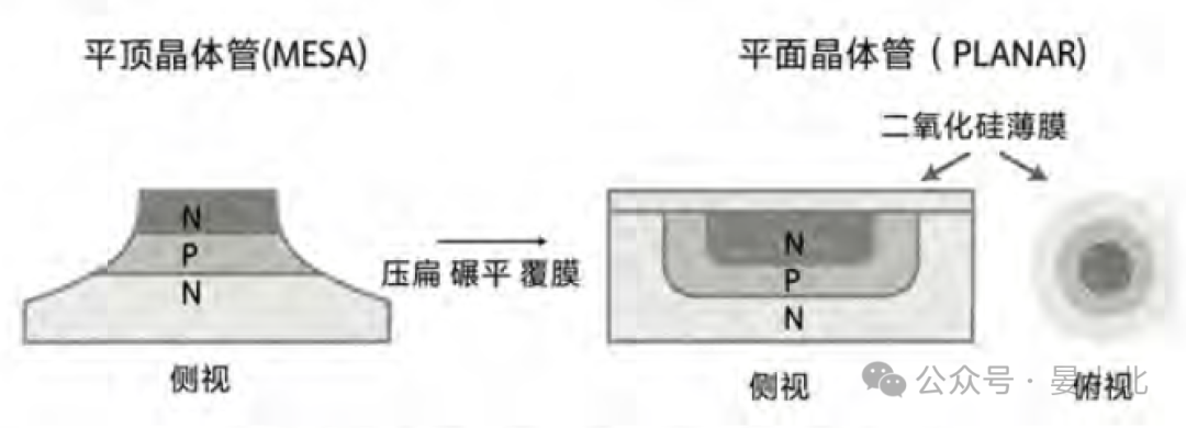
The left image shows the mesa transistor previously used by Fairchild, while the right image shows the planar transistor proposed by Horn.
From top to bottom, they are the emitter, base, and collector.
The core difference between the two lies in the integrity of the semiconductor material.
The mesa transistor resembles a volcano, with a narrow top and a wide base, similar to a “convex” shape,
while the planar transistor is a square piece of semiconductor material, covered with a layer of silicon dioxide film.
The problem with the former is the exposed PN junction sidewalls, which are prone to particle adhesion, reducing device reliability.
This is an inherent defect in the device structure that is difficult to mitigate through production control.
Horn’s idea was to completely flatten this volcano, allowing the narrower top platform to sink into the base.
If viewed from a top-down perspective, this structure is a concentric circle, with the emitter, base, and collector arranged from inside to outside.
After diffusion, a layer of SiO2 film is covered on the surface of the semiconductor material, preventing the PN junction from direct contact with external particles.
Thus, from the perspective of device structure, the reliability issues caused by the exposure of the PN junction are completely resolved.
In March 1959, the first planar transistor was manufactured, and testing showed its reliability far exceeded that of the mesa transistor, which greatly satisfied customers.
Fairchild hired experienced patent attorney John Rawls to prepare a patent application for the planar transistor,
and Rawls felt that the planar transistor idea might have other applications in electronics, so he hoped to write the disclosure in as broad a language as possible.
He told Noyce that Fairchild should make this application as expansive as possible.
“What else can you do with this idea?” This was a question Rawls would remind Noyce of in every discussion.
In the 1950s, it was very difficult to make precise electrical connections between the various regions of an NPN transistor,
because the wires appeared enormous compared to the areas on the chip.
Horn’s planar transistor structure just happened to solve this problem—wires could pass through the SiO2 layer, like candles inserted into a cake, until they reached the surface of the semiconductor.
Furthermore, there was no need for wires at all! You could first open holes in the oxide layer and then print extremely fine metal patterns on the surface of the semiconductor, which is a more convenient industrial process than inserting wires.
By printing metal between the oxide layers, all interconnections can be completed in one go during the transistor manufacturing process.
Moreover, if you can use these metals to connect different regions of a single transistor, why not use this method to interconnect multiple transistors?
Furthermore, why limit it to transistors? If you can build transistors, resistors, and capacitors on a single silicon wafer, why not use this method to achieve interconnections between different components?
This is the embryonic form of the integrated circuit idea conceived by Noyce.
Years later, Noyce admitted that it was Rawls’ question that rescued him from his fixed mindset,allowing him to realize the concept of monolithic integration from a different perspective.
Thus, within six months, Kilby and Noyce each completed this journey—the intellectual journey towards integrated circuits.
However, they took completely different paths,
Kilby was the first to think of constructing all circuit components on a single semiconductor wafer, and as a complement to this concept, he vaguely realized that various components could be connected by “wires” printed on the same wafer.
This was a bottom-up approach,
Noyce, on the other hand, was inspired by the planar transistor and was the first to think of the idea of printing wires on the wafer, which led him to the idea of placing all circuit components on a single chip.
This was a top-down approach.
Different paths leading to the same destination.
On January 23, 1959, just as Kilby was vaguely generating the idea of interconnection, Noyce wrote in his notebook about his conception of the integrated circuit,
Kilby was six months ahead, but the use of the planar process made Noyce’s idea more feasible.
A month later, news reached Silicon Valley that TI was about to announce a brand new circuit that integrated all components onto a single silicon chip to solve the interconnection problem of discrete devices.
This was unsettling news for all companies focused on discrete devices. Their products suddenly faced the threat of obsolescence.
Fairchild immediately held a meeting, and Noyce announced his idea, and the company decided to file a patent immediately.
Noyce could not see Kilby’s patent application document, but he knew that TI would certainly emphasize the revolutionary innovation of “integration” in the application document.
Fairchild had already lost the initiative, and they now needed a patent shield, a patent that could distinguish Noyce’s idea from Kilby’s invention.
Undoubtedly, they needed to emphasize the planar process and interconnection scheme.
Noyce and the lawyers named their application “Semiconductor Device-and-Lead Structure,” focusing on the interconnection scheme,
and the application listed three main purposes of the invention, the first being interconnection—“to provide improved device and lead structures for electrical connections with various semiconductor regions.”
Based on the four-page written description, the lawyer added three pages of images of typical circuits,
which could be integrated onto chips, without flying wires, or even without wires at all.
The structures depicted in these images are not fundamentally different from the integrated circuits produced today.
On July 30, 1959, Fairchild submitted the integrated circuit patent application, choosing the fast-track review process.
Nearly two years later, Fairchild’s application was approved—U.S. Patent No. 2,981,877.
According to the official decree of the United States, Robert N. Noyce—the second person to conceive the idea of monolithic integration—was officially declared the inventor of the integrated circuit.
This was just the beginning, as a nearly 10-year patent lawsuit was about to unfold.
Series of articles on chip history:Chip History—Photolithography and Its OriginsChip History—Kilby’s Decision, The Origin of Integrated CircuitsInventor of the Integrated Circuit—Young KilbyFrom Darwin to KilbyChip History—The Naming of HolesChip History—The Naming of Transistors1958, The Eve of the Invention of Integrated CircuitsThe First Integrated Circuit PatentPlanar Process and Interconnection Issues
Follow Yan Xiaobei to understand chips and the economy.~
Reference: The Chip