【Article Summary】: The BOOM chip will be showcased at HotChips30-2018, demonstrating the complete process from CPU core source code to CPU chip tape-out, validating the idea that the best way to understand a chip is to create it. This creation process begins with chip programming. The article points out that under the RISC-V ecosystem, chip design and development have entered an era characterized by chip programming and agile chip development.
1. The BOOM chip is at HotChips30-2018!
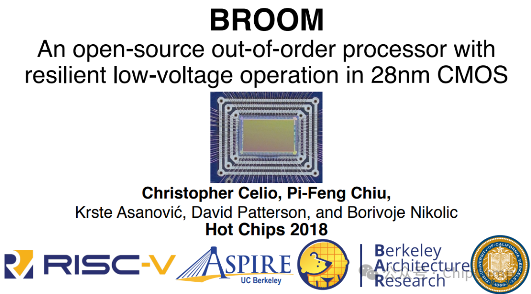
—- Without a tape-out, it would be quite difficult to present at the conference; being able to present posters at HotChips is already commendable.
—- Christopher Celio is probably the person who has written the most BOOM code, as many source files for BOOM are authored by him! Writing code is indeed the correct way to understand a chip, and of course, getting the chip code taped out is also essential! As the saying goes, to understand something, you must create it!
2. Aesthetic Appreciation of the Tape-out!
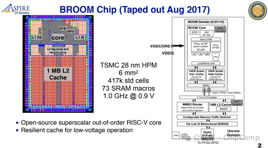
—- The chip size is 2mm * 3mm! Cut from a 12-inch wafer.
—- The first thing to notice is that most of the area is occupied by a 1MB L2 Cache. Then there are the L1 ICache (noted as I$) and L1 DCache (noted as D$), both occupying a regular area. Other regular areas are likely SRAM-type memory! The Core, which is the main logic circuit of the CPU, is not as regular.
—- 417k standard cells (std cells) are a common industry practice to measure circuit logic complexity; each standard cell is approximately equivalent to 0.8 gate circuits and 5 transistors. Therefore, 417K standard cells are roughly equivalent to 333K gate circuits and 2100K (2M) transistors.
—- 73 SRAM macros, which refer to the aforementioned L2 Cache/L1 ICache/L1DCache, are a common industry practice to measure specifications of storage-type (dummy circuits). This is usually not expressed in terms of “how many gate circuits” or “how many transistors”. If one must convert, 73 SRAM macros can be calculated to represent 4M or even more transistors.
—- Previously, I was deeply impressed when hearing about a certain chip having 15 billion transistors. Now, it seems reasonable for chip design professionals to use standard cells (std cells) to reflect the complexity of chip logic; the figure of 15 billion mainly reflects the “chip manufacturing” capability and is used to “intimidate” outsiders, packaging chip design and programming as an exclusive skill.
—- With RISC-V establishing the ecological foundation, whether it is Intel, AMD, ARM, or even Nvidia, there may no longer be any “ecological moat” left; what remains is chip programming representing agile chip development. RISC-V is like Linux from 30 years ago. Go Ahead.
3. Aesthetic Appreciation of the Tape-out:
—- Look at how abstract the CPU Core’s floorplan and Place & Route (P&R) layout are, similar to drawing a map.
—- I$ and D$ refer to ICache and DCache, which is a humorous expression created by industry leaders.
4. Aesthetic Appreciation of the Tape-out:
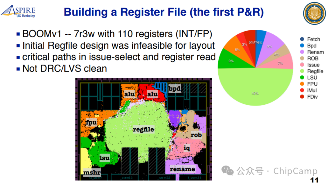
—- This is the aforementioned layout and routing (P&R), mainly reflecting the RegFile and adjacent circuit blocks. As mentioned in previous articles, the RegFile is called a register file, not a register file. Layout refers to the floorplan.
5. Aesthetic Appreciation of the Tape-out:
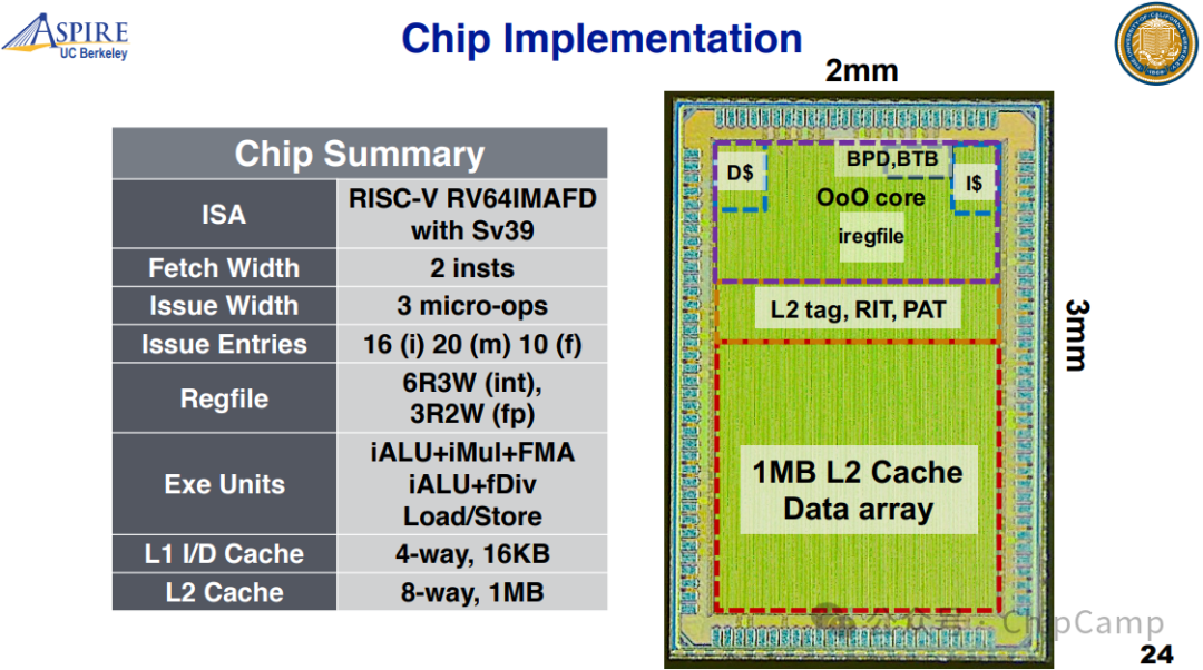
—- There is a high degree of consistency with the previous images. Below is the L2 Cache. The upper left corner is DCache. The upper right corner is ICache. The middle and lower part of the OOO-Core is the RegFile register file.
6. Aesthetic Appreciation of the Tape-out:
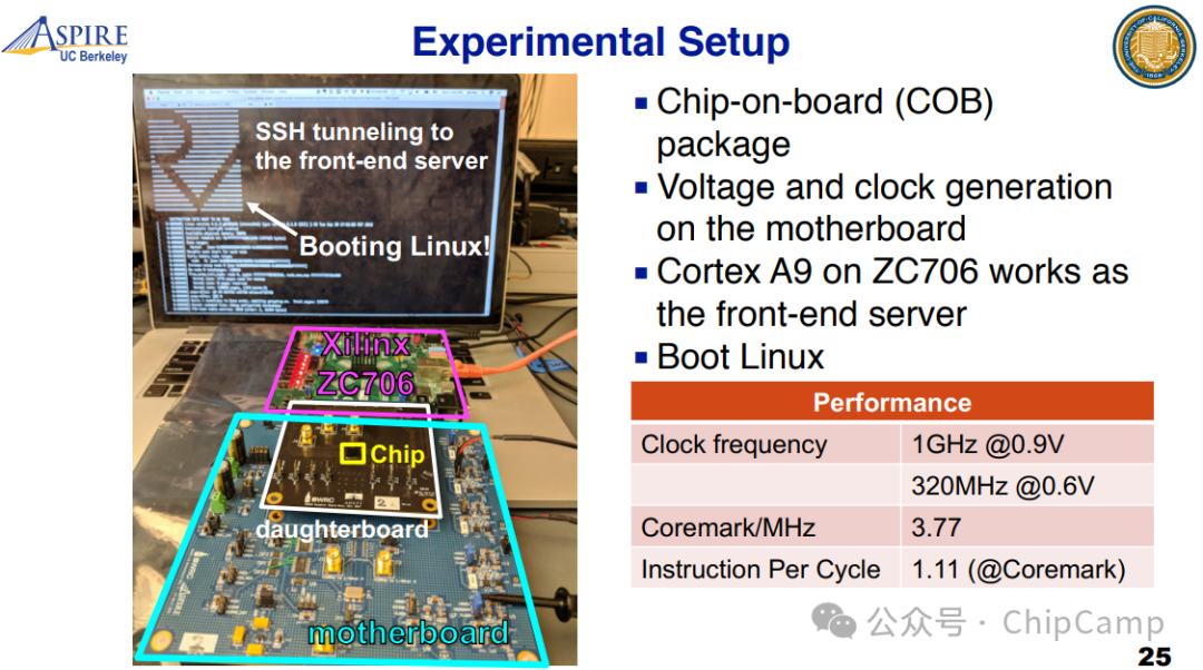
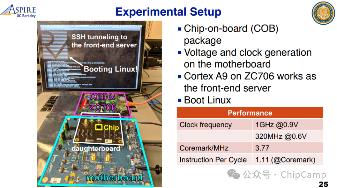
—- Taping out to light up Linux is what makes a CPU chip advanced. If it is just to light up an LED blinking light, that is merely a basic MPU chip, which can be purchased on the market for 3 to 5 dollars, at most 10 dollars. A typical scenario for an MCU is to be used to “light up LED lights”, for example, by monitoring the status of power, network, WiFi, and other chips on a motherboard through I2C, and indicating this status to users through red and green LED lights or blinking. A motherboard has a main CPU running business logic, and also has an MCU to monitor some user components; the MCU is undoubtedly a good tool for practicing CPU programming, but it is relatively basic.
—- The form of a motherboard + core board (daughterboard) is standard for many development boards. Although the core board is small, it contains the core system CPU + DRAM + Flash + IO Controller. The motherboard mainly provides power and peripheral interfaces, replacing manual wiring on the panel board. Of course, it also adds a Xilinx board to form a CPU + FPGA configuration, which is likely used to connect to network cards and displays; connecting the CPU to the FPGA is simpler than connecting the CPU to a bunch of fragmented peripherals.
7. Aesthetic Appreciation of the Tape-out:
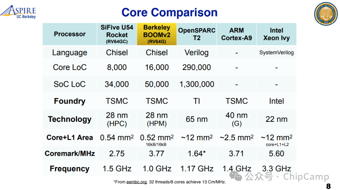
—- A 6 square mm chip, with a 0.52 square mm CPU Core + L1 Cache! But the main Verilog or Chisel code is actually all within this 0.52 square mm!
—- Coremark/MHz is a performance evaluation metric for CPU chips, similar to many other industries’ metrics, CPU design is no exception.
8: Tape-out information mentioned in the 2019 paper:
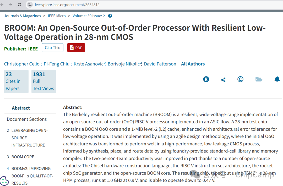
—- The chip tape-out was in 2017. The results of lighting up Linux were presented at the HotChip conference in 2018. The paper was published in 2019.
—- With open-source CPU chip code, tape-out, and lighting up Linux as evidence, the paper has a solid foundation. This is what it means to write a paper on silicon and circuit boards.
9: Tape-out information mentioned in the 2020 SonicBOOM paper:
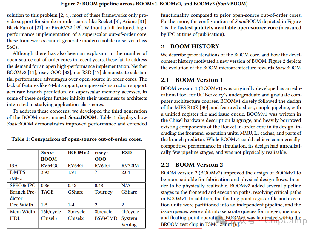
—- It is reiterated that BOOMv2 was fabricated within the BROOM test chip. There is also a small anecdote that BOOMv2 improved the design of BOOMv1 to be more suitable for fabrication and physical design flows. It can be seen that BOOMv1 did not undergo tape-out verification, leading to some deficiencies in the backend physical design, and correspondingly, some shortcomings in the frontend design. This reflects the iterative process of frontend and backend design in chip design.
—- Fortunately, after the tape-out of BOOMv2, there is continued improvement with BOOMv3. The first author of the SonicBOOM (BOOMv3) paper is Jerry Zhao. At this point, Christopher Celio has likely achieved success (PhD graduation) and left Berkeley.
The original text is from the same-named blog on CSDN by this account,this article has been revised.You can click on 【View Original】 at the end of the article to jump to the original text, or browse on PC atChipCamp.blog.csdn.net.