“Integrating an oscilloscope and signal generator into the palm of your hand, all thanks to the STM32G031!”This project utilizes the STM32G031 MCU to collect external audio signals through ADC and DMA, enabling real-time waveform and spectrum display on an OLED screen. Users can adjust parameters such as sampling rate (time axis), amplitude scaling (Y-axis), and trigger modes via buttons. The device also features a built-in signal generator capable of outputting three basic waveforms, with adjustable frequency and amplitude. This project combines fun and practicality, making it an ideal practice project for beginner embedded electronics enthusiasts.
Project Requirements

- Complete the collection of onboard audio signals and waveform display. Sound signal sources can be provided by playing music on a mobile phone or generating audio signals via an app. The waveform is displayed on the OLED screen after amplification by the onboard circuit and collection by the MCU’s ADC. Users can expand or compress the waveform display in two directions (horizontal – time; vertical – amplitude) using the onboard buttons, with customizable button functions.
- Implement the signal generator function, capable of producing sine, triangle, and square waves at frequencies below 2KHz. Users can adjust frequency and amplitude via buttons, and by changing the values of R and C on the board, it can generate analog signals up to 200KHz.
- Measure external analog signals (0-3.3V, DC-200KHz) through the Ain pin, and measure the period and peak-to-peak value of external periodic waveforms.
- Perform FFT transformation on the collected signals and display the fundamental frequency and low-order harmonic components (e.g., 2nd, 3rd, 4th, 5th) on the screen.

Completed Functions and Achieved Performance

1. Waveform Display
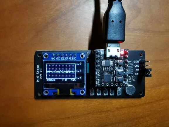
When displaying the waveform, pressing L increases the sampling rate, while pressing R decreases it. The sampling rate can be set to 1kHz, 2.5kHz, 5kHz, 10kHz, 25kHz, 50kHz, 100kHz, 250kHz, 500kHz, or 1MHz, allowing for horizontal scaling of the waveform.
The Y-axis (amplitude range) is set to auto-adjust by default, meaning the program automatically adjusts the Y-axis center voltage and scaling range based on the sampling sequence, ensuring the waveform is fully displayed on the screen. Users can switch to manual mode via the menu to manually adjust the Y-axis center voltage and scaling range.
The lower left corner displays waveform parameters, including time axis scale values, signal peak-to-peak values, DC components, and frequency.
The current status is displayed directly below, including input channel, trigger status, and the aforementioned Y-axis scaling method (A: auto-scaling, MO (Manual Offset): U/D buttons adjust Y-axis center voltage, MS (Manual Scale): U/D buttons adjust Y-axis scaling range).
Pressing the OK button pauses waveform refresh; pressing it again resumes refresh.
2. Trigger Display and Trigger Menu
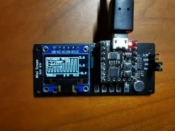
The program defaults to rising edge triggering, with a trigger level of 1.68V. When displaying the waveform with triggering enabled, the current trigger edge (rising edge, falling edge) and trigger status (arrow lit indicates successful trigger, background lit indicates trigger failure) are displayed at the bottom of the screen.
Long-pressing the R button opens the trigger menu, where users can enable/disable triggering, select trigger edge, and choose between auto-triggering or single triggering.
3. Oscilloscope Menu
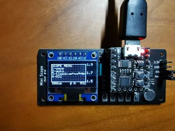
Long-pressing the OK button opens the oscilloscope menu, which contains four options: waveform/spectrum display toggle, Y-axis scaling method, waveform parameter toggle, and channel switch (microphone and onboard signal input). The LRUD buttons are used to switch between these four functions.
4. Spectrum Display
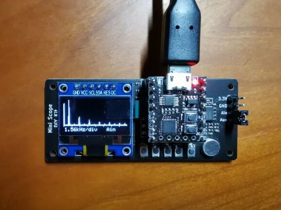
When switching to spectrum display via the menu, the screen shows the signal’s spectrum, with a frequency range from DC to half the sampling frequency. Similarly, pressing L increases the sampling rate, while pressing R decreases it. The lower left corner displays the frequency axis scale values.
5. Signal Output
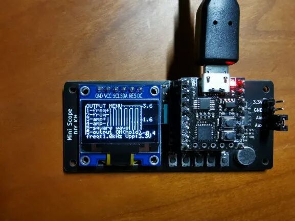
Long-pressing the L button opens the output menu, where users can enable/disable signal output, increase/decrease output signal frequency (step size 100Hz, upper limit 2kHz), peak-to-peak value (step size 0.1V, upper limit 3.3V), and adjust output waveform (sine, triangle, square wave).

Implementation Approach

- ADC samples the analog input, triggered by a timer, with the sampling results transported by DMA.
- The sampled ADC quantization values are mapped to screen coordinates for waveform display.
- Pressing buttons adjusts the sampling frequency, allowing for expansion and compression of the waveform on the time axis.
- Perform FFT transformation on the sampling sequence to draw the spectrum.
- Display signal parameters such as peak-to-peak value, DC component, and signal frequency.
- Output PWM waves and generate square, sine, and triangle waves through RC low-pass filtering. Adjust the PWM frequency and duty cycle via buttons to change the output signal’s frequency and amplitude.

Implementation Process

1. Program Flowchart
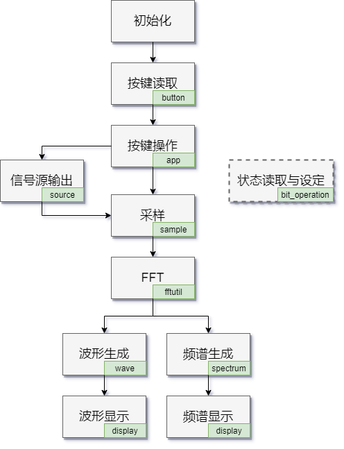
Note: The name in the lower right corner of each block diagram indicates the main file executing that function.
2. ADC Sampling Data
To facilitate FFT calculations, the ADC collects 256 sample points. Each ADC conversion is triggered by Timer 1, with a maximum trigger frequency of 1MHz, meaning the ADC sampling rate can reach up to 1Msps. The ADC conversion results are directly transported to memory by DMA.
/** * @brief Start a new sample sequence. * @param[in] ADCValue Array to store incoming sample values. * @retval None */void start_sample(uint16_t *ADCValue){ HAL_Delay(1); HAL_ADCEx_Calibration_Start(&hadc1); HAL_ADC_Start_DMA(&hadc1, (uint32_t *)ADCValue, SAMPLE_POINTS);}After 256 conversions, an interrupt is triggered, setting the end flag and entering the subsequent data processing program.
ADC conversion complete interrupt callback function (defined in: adc.c):
void HAL_ADC_ConvCpltCallback(ADC_HandleTypeDef *hadc){ if(hadc == &hadc1) { finish_sample(); }}3. Processing Sampling Results
After obtaining 256 sampled ADC quantization values, the waveform starting point is selected based on the trigger level, returning the starting point’s index in the array to display 100 points starting from that index.
Waveform trigger code (defined in: wave.c, called in: app.c, where total_points=256, GRAPH_WIDTH=101):
/** * @brief Wave trigger. * @param[in] ADCValue Array of sampled ADC values. * @param[in] total_points Total sampled points. * @retval Index of the trigger start point(>1). 0 means trigger off or failed. */uint16_t trigger(uint16_t *ADCValue, uint16_t total_points){ uint16_t i; uint16_t trigger_value = VOL2ADC(1.68); if (!is_trigger_on()) return 0; for (i = 1; i < total_points - GRAPH_WIDTH + 2; i++) { if (get_trigger_edge()) // falling edge { if (ADCValue[i-1] > trigger_value && ADCValue[i] <= trigger_value) { trigger_success(); if (is_trigger_single()) pause(); return i; } } else { if (ADCValue[i-1] <= trigger_value && ADCValue[i] > trigger_value) { trigger_success(); if (is_trigger_single()) pause(); return i; } } } trigger_fail(); return 0;}After obtaining the starting point, the next 100 sampled values are displayed on the OLED screen (refreshed all at once). This requires linearly mapping the ADC quantization values to the coordinates on the OLED screen. In auto mode (auto-scaling the Y-axis), the program automatically finds the maximum and minimum values in the quantization values, ensuring that the maximum and minimum values do not exceed the drawing range, allowing the screen to display the complete waveform.
Auto-scaling Y-axis code (defined in: wave.c, called in: app.c):
/** * @brief Automatically find the central/max/min voltage on y-axis. * @param[in] ADCValue Array of sampled ADC values. * @note The function calculates the min/max voltage of the sampled signal, * then find a proper scale voltage and a central voltage on y-axis. * @retval None */void auto_scale(uint16_t *ADCValue){ uint16_t a_max_value, a_min_value, a_pp_value; float exact_voltage, floor_voltage, ceil_voltage; get_max_min_pp_value(ADCValue, &a_max_value, &a_min_value, &a_pp_value); voltage_range_auto_select(ADC2VOL(a_pp_value/2)); exact_voltage = ADC2VOL(a_max_value + a_min_value) / 2; floor_voltage = (uint8_t)(ADC2VOL((a_max_value + a_min_value)*5)) / 10.0; //keep one decimal ceil_voltage = floor_voltage + 0.1; // round center_voltage volt_on_y_axis.center_voltage = ceil_voltage - exact_voltage < exact_voltage - floor_voltage ? ceil_voltage : floor_voltage; volt_on_y_axis.max_voltage = volt_on_y_axis.center_voltage + v_scale_list[v_scale_index]; volt_on_y_axis.min_voltage = volt_on_y_axis.center_voltage - v_scale_list[v_scale_index];}Coordinate mapping code (defined in: wave.c, called in: app.c):
/** * @brief Generate y-coordinates of the wave. * @param[in] ADCValue Array of sampled ADC values. * @param[out] y Y-coordinate array of the wave. * @note The function map ADCValues to OLED y coordinates. * @retval None */void generate_wave(uint16_t *ADCValue, uint8_t *y){ // Quantize y-axis min/max/central voltages to ADC values. int16_t a_max_value = VOL2ADC(volt_on_y_axis.max_voltage); int16_t a_min_value = VOL2ADC(volt_on_y_axis.min_voltage); uint8_t i; // Linearly map every ADC value to its coordinate. for (i = 0; i < GRAPH_WIDTH - 1; i++) { if (ADCValue[i] <= a_max_value && ADCValue[i] >= a_min_value) y[i] = (GRAPH_HEIGHT - 1) * (a_max_value - ADCValue[i]) / (a_max_value - a_min_value) + GRAPH_START_Y; else if (ADCValue[i] > a_max_value) y[i] = GRAPH_START_Y; else if (ADCValue[i] < a_min_value) y[i] = GRAPH_HEIGHT + GRAPH_START_Y - 1; }}Waveform display code (defined in: display.c, called in: app.c):
/** * @brief Display wave on OLED. * @param[in] y Y-coordinate array of the wave. * @retval None */void display_wave(const uint8_t *y){ uint8_t x; for (x = GRAPH_START_X; x < GRAPH_WIDTH - 1; x++) OLED_DrawLine(x, y[x-GRAPH_START_X], x + 1, y[x-GRAPH_START_X+1], 1); OLED_DrawPoint(x, y[x-GRAPH_START_X], 1);}In manual mode, users can manually adjust the Y-axis scaling range and Y-axis center voltage value, but the waveform may not be fully displayed. After obtaining the sampled point coordinates, the OLED’s line drawing function is used to connect the discrete points on the screen, resulting in the signal’s waveform.
When displaying the spectrum, all ADC quantization values undergo a 256-point FFT transformation. Since the FFT transformation results are symmetric about the center point, and the screen’s x-direction resolution is 128 points, only the results from 0 to 127 are retained and displayed on the screen after linear mapping.
The FFT code is defined in fftutil.c, while the processing and display of the transformation results are defined in spectrum.c and display.c, respectively.
4. Signal Generator
A low-pass filter composed of a 1Kohm resistor and a 10nF capacitor on the board has a cutoff frequency of 1.6KHz. If a sufficiently high-frequency PWM signal is output at this terminal, the output voltage will be proportional to the PWM duty cycle. By changing the PWM duty cycle, the output voltage waveform can be adjusted. Experiments show that when each cycle of the signal consists of 500 PWM pulses, the ripple is minimal.
For example, to generate a sine signal, a sine signal is generated externally on a computer, and 500 samples are taken within one cycle. The duty cycle of the 500 PWM pulses can be calculated based on the voltage and PWM duty cycle’s proportional relationship. This is defined as an array of length 500 written into the program. The program enables the PWM DMA channel, allowing the elements of the array to be automatically loaded into the timer output compare register after each PWM pulse, thus changing the duty cycle. The low-pass filter then converts the PWM pulses generated by the STM32 into an analog signal, thereby regenerating the sine wave. The same principle applies to square and triangle waves.
Code to enable PWM and DMA (defined in: source.c, called in: app.c, where SIGNAL_LENGTH=500):
/** * @brief Start signal output at Aux. * @retval None */void start_output(void){ HAL_TIM_PWM_Start_DMA(&htim2, TIM_CHANNEL_2, (uint32_t *)output_wave_value, SIGNAL_LENGTH);}Amplitude adjustment of the signal can be achieved by multiplying each element of the above array by a constant. Frequency adjustment requires first changing the timer’s auto-reload value (ARR) to alter the PWM frequency. To maintain the amplitude, each element in the array must also be scaled proportionally.

Main Challenges Encountered

1. Interrupts and DMA
The project uses DMA in two places: to store ADC sampling results and to adjust the PWM timer’s auto-reload value (ARR). If interrupts were used to handle data instead of DMA, the following issues would arise:
If the conversion result is read in the ADC conversion complete interrupt, the interrupt frequency would be too high during a single sampling sequence (256 points), and due to the time taken by the interrupt, a high sampling rate could not be achieved, with a maximum of only tens of kHz. Using DMA allows the interrupt to be triggered only after the entire sampling sequence is complete, without affecting the sampling.
If the PWM interrupt is used to update the auto-reload value, the time taken by the interrupt would cause deviations in the PWM frequency and affect the SPI timing of the OLED screen, leading to display issues. Using DMA to update the auto-reload value eliminates the need for PWM interrupts, significantly improving update time compared to interrupts.
In summary, in situations requiring high frequency or frequent data updates, interrupts can cause various issues, while DMA can efficiently complete tasks.
2. RAM and Flash Size (FFT Optimization)
The FFT algorithm used in this project is modified from Adafruit ZeroFFT. This algorithm supports up to 4096-point FFT, but its rotation factor table, window function table, and signal sequence array occupy a significant amount of space. The STM32G031G8 used in this project has only 64K of Flash and 8K of RAM, which is extremely limited and cannot directly run ZeroFFT.
Therefore, optimization of the ZeroFFT code is necessary. This project only requires 256-point FFT, so removing parts beyond 256 points and shortening the lookup table can greatly reduce RAM and Flash usage.
Specific optimization steps:
- Change the macro definition ZERO_FFT_MAX in Adafruit_ZeroFFT.h to 512 (for 256-point FFT).
- Remove all other point FFT code from the ZeroFFT function in fftutil.c, keeping only the 256-point FFT code. Similarly, remove parts of the window function beyond 256 points and the window function lookup table.
- At this point, fftutil.c only calls arm_common_tables.c for armBitRevTable and twiddleCoefQ15 lookup tables, removing all other arrays.
- Add printf statements below the code that calls armBitRevTable and twiddleCoefQ15 lookup tables in fftutil.c to print the indices called when running the FFT program on a PC.
- For example, the original length of the twiddleCoefQ15 array is 6144; for 256-point FFT, only 384 values are called. Write a temporary program on the PC to print a new lookup table of length 384 based on the called indices, replacing the original. The same applies to the other lookup table.
- Some variables in fftutil.c represent the step values of the lookup tables; these step values must also be changed after the lookup tables are modified.
- At this point, the FFT code should be able to run on the STM32G0.
Additionally, due to limited Flash and RAM resources, many other areas outside of FFT also require space optimization, such as removing unnecessary font libraries for the OLED.
3. PWM Output Power
Due to the charging and discharging of the capacitor, the signal output through the low-pass filter from PWM will have a sawtooth shape, which is more pronounced at lower signal amplitudes and can cause instability in waveform display. Initially, the output signal had 50 PWM pulses per cycle, meaning the PWM frequency was 50 times the signal frequency. At lower signal amplitudes, the sawtooth effect was very noticeable, causing significant interference with the output waveform. Increasing the number of PWM pulses per cycle to 500 reduces the sawtooth density and, consequently, the interference with the output signal. However, this also increases the size of the lookup table storing the output signal amplitude information by tenfold, consuming more space.

Future Plans and Suggestions

This project has successfully implemented the functions of a simple oscilloscope and signal generator, achieving the expected targets. However, there are many areas for improvement and expansion by changing hardware:
- The OLED screen on the board has a low resolution, making it difficult to display signal details and more information. A higher resolution screen could be used, or waveform information could be sent directly to a host computer for display.
- The resources of the STM32G031 microcontroller are limited. A better microcontroller could be used to improve sampling rates, number of samples, and achieve higher performance.
- Input signals could be attenuated to increase the input signal voltage range.
- Additional analog input channels could be added, along with mathematical operations for waveforms, such as addition and subtraction between waveforms.
- Changing the RC values at the output could extend the output signal frequency range.
There are also areas for improvement and expansion without changing hardware (parts that are less desirable to implement):
- Automatic/manual adjustment of trigger levels.
- Changing the input signal coupling method (DC/AC coupling).
- Digital filtering of input signals.
- Achieving higher frequency resolution for the signal source.

Click “Read Original” to view the project.