This article is approximately 4,500 words long, recommended for saving and reading.
Author | Engineer Xiao Mo
Produced by | Automotive Electronics and Software
Welcome to follow the public account belowAbao1990, this public account focuses on autonomous driving and smart cockpits, providing you with automotive insights every day. We start with cars, but we are not limited to cars.

Table of Contents
1. Introduction
2. Basic Theory of SPI Protocol
3. Hardware Design Solutions
4. Software Architecture Design
5. Driver Implementation
6. Summary
1. Introduction
1.1 Document Background
The Serial Peripheral Interface (SPI) is a full-duplex synchronous serial communication interface developed by Motorola, widely used for data transmission between microcontrollers and peripheral devices. This document uses the communication between MCU and FLASH memory as an example to elaborate on the hardware design, software implementation, and practical applications of SPI communication.
1.2 Application Scenarios
SPI communication plays an important role in embedded systems, mainly applied in:
-
Communication between microcontrollers and memory (FLASH,EEPROM)
-
Sensor data acquisition (temperature, pressure, acceleration sensors)
-
Display driver (LCD,OLED)
-
ADC/DAC converter control
-
Real-time clock (RTC) module communication
1.3 Technical Advantages
Compared to other communication protocols, SPI has the following advantages:
-
High-speed transmission: Clock frequencies can reach tens of MHz
-
Full-duplex communication: Simultaneous data transmission and reception
-
Simple hardware: Only requires4 signal lines
-
High flexibility: Supports multiple slave devices in a daisy chain
2. Basic Theory of SPI Protocol
2.1 Protocol Architecture
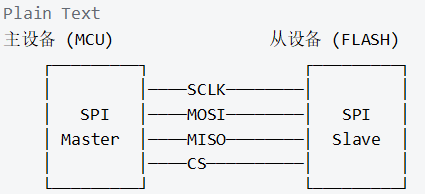
SPI adopts a master-slave architecture, where one master device can control multiple slave devices. Communication is based on a clock synchronization mechanism, and data transmission strictly follows the clock pulse.
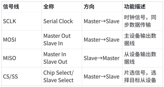
2.2 Signal Line Definitions
2.3 Working Timing
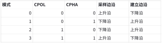
The core of SPI communication is the configuration of clock polarity (CPOL) and clock phase (CPHA):
2.3.1 Clock Polarity (CPOL)
-
CPOL=0: In idle state,SCLK is low
-
CPOL=1: In idle state,SCLK is high
2.3.2 Clock Phase (CPHA)
-
CPHA=0: Sample data on the first edge ofSCLK
-
CPHA=1: Sample data on the second edge ofSCLK
2.3.3 Four Working Modes
3. Hardware Design Solutions
3.1 System Architecture Design
The entire system consists of three core modules:MCU main controller, SPI communication interface, FLASH memory.
Core Module Description:
-
MCU Module:STM32F407 serves as the main controller, responsible for the control logic of the entire system
-
SPI Module: Four-wire communication interface(SCLK/MOSI/MISO/CS), achieving high-speed data transmission
-
FLASH Module:W25Q64 provides8MB of non-volatile storage space
3.2 Pin Connection Scheme
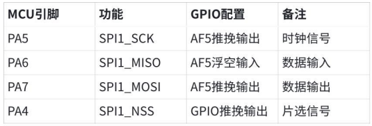
3.2.1 MCU Pin Configuration (using SPI1)
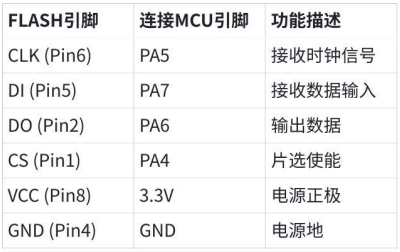
3.2.2 FLASH Pin Connection
3.3 Circuit Design Points
3.3.1 Power Design
Plain TextVCC (3.3V) ──┬── 100nF ──┬── GND │ └── W25Q64 VCC3.3.2 Signal Integrity Design
-
Pull-up Resistor:CS signal adds a10kΩ pull-up resistor to ensure default high level
-
Decoupling Capacitor:FLASH power supply adds a100nF decoupling capacitor
-
Trace Impedance: High-speed signal lines are controlled at50Ω characteristic impedance
-
Trace Length: SPI signal line length matching, maximum difference<5mm
4. Software Architecture Design
4.1 System Software Architecture
The software architecture adopts a simple three-layer design:
Architecture Level Description:
-
Application Layer: Implements specific business functions, such as data recording, querying, etc.
-
Driver Layer: Encapsulates SPI communication and FLASH operations, providing a unified interface
-
Hardware Layer: Based on STM32 HAL library, handling low-level hardware operations
4.2 Module Design
4.2.1 SPI Driver Module Interface Design
Based on STM32 HAL library, the SPI driver module mainly includes configuration structures and basic operation interfaces:
C// SPI configuration structuretypedef struct {uint32_t baudrate; // Baud rateuint8_t mode; // Operating mode (0-3)uint8_t data_size; // Data size (8/16)uint8_t cs_pin; // Chip select pin} spi_config_t;// SPI driver interfaceHAL_StatusTypeDef SPI_Init(spi_config_t* config);HAL_StatusTypeDef SPI_Transmit(uint8_t* data, uint16_t size);HAL_StatusTypeDef SPI_Receive(uint8_t* data, uint16_t size);HAL_StatusTypeDef SPI_TransmitReceive(uint8_t* tx_data, uint8_t* rx_data, uint16_t size);HAL_StatusTypeDef SPI_DeInit(void);Interface Design Points::
-
Configuration Structure: Contains key parameters such as baud rate, operating mode, data size, and chip select pin
-
Initialization Interface: Completes the configuration of SPI peripherals and GPIO settings
-
Data Transmission Interface: Supports sending, receiving, and bidirectional transmission
-
Error Handling Mechanism: Provides unified status return and error handling
4.2.2 FLASH Driver Module Interface Design
Designed for W25Q64 device characteristics:
C// FLASH device information structuretypedef struct {uint32_t sector_size; // Sector size (4KB)uint32_t block_size; // Block size (64KB)uint32_t total_size; // Total capacity (8MB)uint16_t manufacturer_id; // Manufacturer ID (0xEF)uint16_t device_id; // Device ID (0x4017)uint8_t unique_id[8]; // Unique identifier} w25q64_info_t;// FLASH operation interfaceHAL_StatusTypeDef W25Q64_Init(void);HAL_StatusTypeDef W25Q64_ReadID(w25q64_info_t* info);HAL_StatusTypeDef W25Q64_ReadData(uint32_t address, uint8_t* data, uint32_t size);HAL_StatusTypeDef W25Q64_WritePage(uint32_t address, uint8_t* data, uint32_t size);HAL_StatusTypeDef W25Q64_EraseSector(uint32_t address);HAL_StatusTypeDef W25Q64_EraseBlock(uint32_t address);HAL_StatusTypeDef W25Q64_EraseChip(void);HAL_StatusTypeDef W25Q64_ReadStatus(uint8_t* status);uint8_t W25Q64_IsBusy(void);Interface Design Points::
-
Device Information Structure: Stores information such as FLASH capacity, sector size, manufacturer ID, etc.
-
Basic Operation Interface: Includes initialization, read ID, data read/write, sector erase, etc.
-
Address Management: Supports complete access to 24-bit address space
-
Status Detection: Implements busy status detection and write protection management
5. Driver Implementation
5.1 SPI Communication Driver Implementation
The core task of the SPI driver is to enable the MCU and FLASH to “communicate“. Just like two people making a phone call need to follow communication etiquette, the communication between MCU and FLASH also needs to follow the SPI protocol.
5.1.1 SPI Initialization – Establishing Communication Connection
Imagine the MCU wants to call the FLASH, first it needs to:
1. Open the phone line (enable clock)
2. Configure the phone (set GPIO pins)
3. Agree on the communication method (configure SPI parameters)
C#include "stm32f4xx_hal.h"static SPI_HandleTypeDef hspi1; // SPI's "phone"HAL_StatusTypeDef SPI_Init(void){// Step 1: Open the "phone line" - enable clock __HAL_RCC_GPIOA_CLK_ENABLE(); // GPIO clock __HAL_RCC_SPI1_CLK_ENABLE(); // SPI clock// Step 2: Connect the "phone line" - configure pins GPIO_InitTypeDef GPIO_InitStruct = {0};// Data line configuration (SCK, MISO, MOSI) GPIO_InitStruct.Pin = GPIO_PIN_5 | GPIO_PIN_6 | GPIO_PIN_7; GPIO_InitStruct.Mode = GPIO_MODE_AF_PP; // Multiplex push-pull output GPIO_InitStruct.Speed = GPIO_SPEED_FREQ_VERY_HIGH; // High-speed mode GPIO_InitStruct.Alternate = GPIO_AF5_SPI1; // Select SPI1 function HAL_GPIO_Init(GPIOA, &GPIO_InitStruct);// Chip select line configuration (CS) GPIO_InitStruct.Pin = GPIO_PIN_4; GPIO_InitStruct.Mode = GPIO_MODE_OUTPUT_PP; // Normal output GPIO_InitStruct.Pull = GPIO_PULLUP; // Pull-up, default high level HAL_GPIO_Init(GPIOA, &GPIO_InitStruct);// Step 3: Set the "communication rules" - configure SPI parameters hspi1.Instance = SPI1; // Use SPI1 hspi1.Init.Mode = SPI_MODE_MASTER; // MCU is the master hspi1.Init.DataSize = SPI_DATASIZE_8BIT; // Send 8 bits of data each time hspi1.Init.CLKPolarity = SPI_POLARITY_LOW; // Clock is low in idle state hspi1.Init.CLKPhase = SPI_PHASE_1EDGE; // Sample on the first edge hspi1.Init.BaudRatePrescaler = SPI_BAUDRATEPRESCALER_4; // Speed: 42MHz÷4=10.5MHzreturn HAL_SPI_Init(&hspi1); // Start the "phone system"}Key Parameter Explanation:
-
Clock Prescaler: Just like adjusting the call speed, a larger prescaler slows down the speed but makes it more stable
-
Polarity and Phase: Determine when to“speak” and when to“listen”.
-
Chip Select Signal: Equivalent to a phone number, determines who to call
5.1.2 Data Transmission – The Actual“Call” Process
Data transmission is like the process of making a phone call:
1. Dialing (pulling down CS signal)
2. Talking (sending/receiving data)
3. Hanging up (pulling up CS signal)
C// Define "dialing" and "hanging up" operations#define FLASH_CALL_START() HAL_GPIO_WritePin(GPIOA, GPIO_PIN_4, GPIO_PIN_RESET) // Dial#define FLASH_CALL_END() HAL_GPIO_WritePin(GPIOA, GPIO_PIN_4, GPIO_PIN_SET) // Hang up// Bidirectional call - MCU both speaks and listensHAL_StatusTypeDef SPI_Chat(uint8_t* send_data, uint8_t* receive_data, uint16_t length){ HAL_StatusTypeDef status; FLASH_CALL_START(); // Start call// Simultaneously send and receive data (full-duplex communication) status = HAL_SPI_TransmitReceive(&hspi1, send_data, receive_data, length, 1000); FLASH_CALL_END(); // End callreturn status;}// Unidirectional send - only speak, not listenHAL_StatusTypeDef SPI_Tell(uint8_t* data, uint16_t length){ HAL_StatusTypeDef status; FLASH_CALL_START(); // Dial status = HAL_SPI_Transmit(&hspi1, data, length, 1000); // Send command FLASH_CALL_END(); // Hang upreturn status;}// Unidirectional receive - only listen, not speakHAL_StatusTypeDef SPI_Listen(uint8_t* data, uint16_t length){ HAL_StatusTypeDef status; FLASH_CALL_START(); // Dial status = HAL_SPI_Receive(&hspi1, data, length, 1000); // Receive data FLASH_CALL_END(); // Hang upreturn status;}Communication Points:
-
CS Signal: Just like dialing a phone, you must dial before you can talk
-
Timeout Settings:1000ms timeout to avoid the program“hanging”
-
Full Duplex: SPI can send and receive simultaneously, just like chatting face to face
5.2 FLASH Memory Driver Implementation
FLASH is like a smart storage cabinet, the MCU needs to use a specific“password” (command) to operate it.
5.2.1 FLASH‘s“Password Book” – Command Set
Just like different remote control buttons have different functions, FLASH also has its own command set:
C// FLASH's "password book" - various operation commands#define CMD_READ_ID 0x9F // "Who are you?" - Check ID#define CMD_READ_DATA 0x03 // "Give me the data" - Read data #define CMD_WRITE_ENABLE 0x06 // "I want to write something" - Request write permission#define CMD_PAGE_WRITE 0x02 // "Store this data" - Write data#define CMD_SECTOR_ERASE 0x20 // "Clear this area" - Erase 4KB#define CMD_CHIP_ERASE 0xC7 // "Clear everything" - Erase the entire chip#define CMD_READ_STATUS 0x05 // "Are you busy?" - Query status// FLASH's "status light" - meaning of each bit in the status register#define STATUS_BUSY 0x01 // Busy flag: 1=working, 0=idle#define STATUS_WRITE_ENABLE 0x02 // Write enable flag: 1=can write, 0=write prohibitedUnderstanding Command Classification:
-
Identity Class:READ_ID – Confirm FLASH model to prevent misidentification
-
Read Class:READ_DATA – Read data from the specified address
-
Write Class:WRITE_ENABLE + PAGE_WRITE – Request permission before writing data
-
Erase Class:SECTOR_ERASE, CHIP_ERASE – Delete data (must erase before writing)
-
Status Class:READ_STATUS – Query FLASH whether it is busy
5.2.2 Basic Operations – Daily Communication with FLASH“
Implementing basic functions to communicate with FLASH is like common phrases in daily conversation:
C// "Are you busy?" - Wait for FLASH to be freestatic HAL_StatusTypeDef Flash_WaitFree(void){ uint8_t status; uint32_t patience = 1000; // Be patient for 1000 millisecondsdo {// Ask FLASH: "Are you busy?" FLASH_CALL_START(); uint8_t ask_cmd = CMD_READ_STATUS; HAL_SPI_Transmit(&hspi1, &ask_cmd, 1, 100); HAL_SPI_Receive(&hspi1, &status, 1, 100); FLASH_CALL_END();// If FLASH answers "not busy" (BUSY bit is 0)if (!(status & STATUS_BUSY)) { return HAL_OK; // Can continue operation } HAL_Delay(1); // Wait 1 millisecond patience--; } while (patience > 0); return HAL_TIMEOUT; // Waited too long, give up}// "I want to write something" - Request write permission static HAL_StatusTypeDef Flash_AskPermission(void){ uint8_t permit_cmd = CMD_WRITE_ENABLE; FLASH_CALL_START(); HAL_StatusTypeDef result = HAL_SPI_Transmit(&hspi1, &permit_cmd, 1, 100); FLASH_CALL_END(); return result;}// "Who are you?" - Read FLASH IDHAL_StatusTypeDef Flash_CheckID(void){ uint8_t ask_id_cmd = CMD_READ_ID; uint8_t id_card[3]; // FLASH's 3-byte ID card HAL_StatusTypeDef status; FLASH_CALL_START();// Ask: "Who are you?" status = HAL_SPI_Transmit(&hspi1, &ask_id_cmd, 1, 100); if (status != HAL_OK) { FLASH_CALL_END(); return status; }// Listen to FLASH's answer for ID status = HAL_SPI_Receive(&hspi1, id_card, 3, 100); FLASH_CALL_END(); if (status == HAL_OK) {// Interpret ID carduint8_t manufacturer = id_card[0]; // Manufacturer IDuint16_t device_type = (id_card[1] << 8) | id_card[2]; // Device type// Verify if it is the expected W25Q64if (manufacturer == 0xEF && device_type == 0x4017) { printf("Found W25Q64 FLASH! Capacity: 8MB\n"); return HAL_OK; } else { printf("Error: This is not a W25Q64 chip\n"); return HAL_ERROR; } } return status;}Operation Points:
-
Be Patient: FLASH will be busy during erase or write, so be patient
-
Request Permission First: Must send write enable command before writing
-
Verify Identity: Confirm chip model through ID to avoid misoperation
5.2.3 Data Read/Write – The Real“Access” Operation
Data read/write is like going to the bank to deposit or withdraw money, requiring accurate address information:
C// "Give me the data at address X" - Read dataHAL_StatusTypeDef Flash_ReadData(uint32_t address, uint8_t* buffer, uint32_t size){ HAL_StatusTypeDef status; uint8_t command_packet[4]; // Command packet: 1 byte command + 3 bytes address// Safety check: address cannot exceed FLASH capacityif (address + size > 0x800000) { // 8MB capacity limitprintf("Error: Read address out of range\n"); return HAL_ERROR; }// Wait for FLASH to be free status = Flash_WaitFree(); if (status != HAL_OK) return status;// Prepare "read" command packet command_packet[0] = CMD_READ_DATA; // Command: "Give me data" command_packet[1] = (address >> 16) & 0xFF; // High byte of address command_packet[2] = (address >> 8) & 0xFF; // Middle byte of address command_packet[3] = address & 0xFF; // Low byte of address FLASH_CALL_START();// First say the address status = HAL_SPI_Transmit(&hspi1, command_packet, 4, 1000); if (status != HAL_OK) { FLASH_CALL_END(); return status; }// Then receive data status = HAL_SPI_Receive(&hspi1, buffer, size, 1000); FLASH_CALL_END(); if (status == HAL_OK) { printf("Successfully read %lu bytes from address 0x%06lX\n", size, address); } return status;}// “Store this data at address X” – Write data (page programming)
CHAL_StatusTypeDef Flash_WriteData(uint32_t address, uint8_t* data, uint32_t size){ HAL_StatusTypeDef status; uint8_t command_packet[4]; // Command packet// FLASH write rules: maximum of 256 bytes can be written at once (one page), and cannot cross pagesif (size > 256 || (address & 0xFF) + size > 256) { printf("Error: Writing data exceeds page boundary\n"); return HAL_ERROR; }// Step 1: Wait for FLASH to be free status = Flash_WaitFree(); if (status != HAL_OK) return status;// Step 2: Request write permission (a necessary courtesy) status = Flash_AskPermission(); if (status != HAL_OK) return status;// Step 3: Prepare write command packet command_packet[0] = CMD_PAGE_WRITE; // Command: "I want to write data" command_packet[1] = (address >> 16) & 0xFF; // Target address high byte command_packet[2] = (address >> 8) & 0xFF; // Target address middle byte command_packet[3] = address & 0xFF; // Target address low byte FLASH_CALL_START();// Step 4: Send command and address status = HAL_SPI_Transmit(&hspi1, command_packet, 4, 1000); if (status != HAL_OK) { FLASH_CALL_END(); return status; }// Step 5: Send actual data status = HAL_SPI_Transmit(&hspi1, data, size, 1000); FLASH_CALL_END();// Step 6: Wait for FLASH to complete writing (writing takes time)if (status == HAL_OK) { status = Flash_WaitFree(); // Be patient while waiting for writing to completeif (status == HAL_OK) { printf("Successfully wrote %lu bytes to address 0x%06lX\n", size, address); } } return status;}Important Rules for Writing to FLASH:
-
Erase before Write: FLASH can only change1 to0, to write, it must be erased first
-
Page Write: Maximum of 256 bytes can be written at once, cannot cross pages
-
Write Permission: Must request write enable before each write
-
Be Patient: Writing takes a few milliseconds
6. Summary
This document introduces a complete implementation plan for SPI communication technology:
-
Basic Knowledge of SPI: SPI is a 4-wire communication protocol, including clock line(SCLK), data output line(MOSI), data input line(MISO), and chip select line(CS).
-
Hardware Connection: Using STM32F407‘s PA4-PA7 pins to connect to the W25Q64 FLASH chip, achieving communication between MCU and memory.
-
Software Implementation: Configuring SPI peripherals using HAL library, writing driver functions to implement read, write, and erase operations for FLASH.
-
Practical Applications: After mastering the content of this document, you can flexibly use SPI interface to connect various peripheral devices in projects.
SPI communication is simple and reliable, an important technology in embedded development. Through theoretical learning and practical programming, it can be quickly mastered and applied in real projects.
A group of like-minded friends gather in the Knowledge Star Sphere
Join “Abao Talks Cars” Knowledge Sphere to obtain relevant learning materials for these modules (currently includes research reports, online expert sharing, offline closed-door meetings), covering 16 major sections, detailed list as follows: