▲ Click☆Star me to avoid losing contact

In modern vehicles, numerous Electronic Control Units (ECUs) are responsible for controlling various functions such as engine management, transmission control, braking systems, and infotainment systems. Each ECU typically comes equipped with its own MCU, which increases the overall complexity and cost of the vehicle’s electrical architecture.
The situation is similar for vehicle lighting, where the front, rear, and side lights usually have their own independent ECUs. Especially in cases where some lights contain hundreds or thousands of pixels, or when the lights are composed of multiple distributed printed circuit boards (PCBs), each light board requires an MCU as a control forwarding point to enhance system reliability, communication speed, and electromagnetic compatibility (EMC) performance, given the abundance of mass-produced LED driver solutions available in the market.
This article presents a solution using the TLD7002-16ES as an example, proposing a cost-reduction strategy and improved EMC performance through a UART OVER CAN communication interface.
Introduction
The TLD7002-16ES is a 16-channel automotive LED constant current source driver chip, equipped with comprehensive protection and diagnostic features, supporting UART, OVRE, and CAN protocols with communication rates of up to 2M. This chip is designed to control LED currents of up to 76.5 mA and operates as a linear current sink (LCS). By paralleling the power output stages, higher load currents can be achieved. Each independent power output stage is configured with a 6-bit current setting value stored in OTP and supports 16 independent PWM configurations. A high-speed lighting interface is used for OTP programming, configuration, control, and diagnostic feedback. This chip can directly drive multi-pixel LEDs, eliminating the need for additional MCUs on the light boards.
Additionally, the TLD7002-16ES can serve as a gateway to control other external LED drivers, such as linear constant current sources (Infineon LITIX™ Basic+ series) or DC/DC converters (LITIX™ Power). Without the need for additional MCUs, existing solutions can be retained, and even the number of UART OVER CAN linear LED driver chips can be reduced, thereby supporting higher system output currents. This approach effectively optimizes system costs.
Gateway Method Advantages
-
Integrates the UART over CAN interface into existing LED drivers.
-
Removes the microcontroller from the LED driver unit.
-
Enhances the current capability of the TLD7002-16ES, including increased channel count and maximum current.
-
Optimizes thermal management performance by distributing heat among multiple LED drivers.
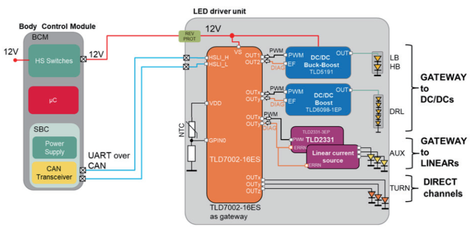
Figure 1: Example of TLD7002-16ES Gateway Implementation
When using the TLD7002-16ES as a gateway to control external LED drivers, the following connections are required:
-
The OUTn channels of the TLD7002-16ES provide PWM signals to the external LED drivers.
-
The diagnostic function is based on the Fault/ERR pin of the external LED driver. The Fault pin is sampled by the OUTn channel of the TLD7002-16ES or the adjacent OUTn+1 channel, depending on specific application requirements.
Thus, a “gateway channel” may occupy two outputs of the TLD7002-16ES: one for PWM and one for diagnostics.
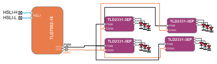
Figure 2: Connection of External LED Driver and Adjacent Channels of TLD7002-16ES
When multiple linear current sources are connected to a single PWM output, and the Fault pin collects from one TLD7002-16ES output, the total output channel usage of the TLD7002-16ES can be halved.
In some cases, a single TLD7002-16ES channel can serve both PWM and diagnostic purposes simultaneously through simple workarounds.
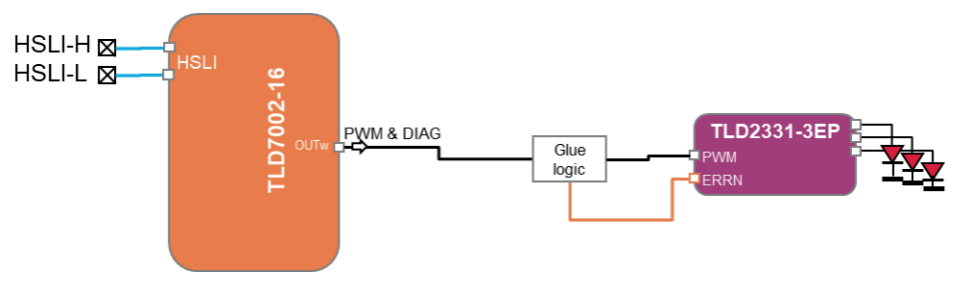
Figure 3: Merging PWM and Diagnostics on a Single Output of TLD7002-16ES
Key Points for Gateway Design Based on TLD7002-16ES
Generating PWM with TLD7002-16ES
The TLD7002-16ES is a low-side open-drain current sink, thus the PWM it generates is inverted. This inverted PWM signal can be easily managed through software, but a better approach is to generate a high-level PWM when the TLD7002-16ES is sinking current (i.e., when the TLD7002-16ES output is enabled). Maintaining inverted PWM may produce unwanted spikes at the output of the external LED driver.
The inversion of the PWM signal can be achieved using a simple BJT transistor, as shown in Figure 4. To reduce power loss, the current setting of the OUT12 channel of the TLD7002-16ES can be set to a minimum (5.6 mA). Additionally, using a 10 kΩ resistor at the base can further reduce power loss. However, this may lead to false open-loop (OL) detection and current warnings on the OUT12 channel, which the application software must ignore. Alternatively, the base resistor R78 can be set to a lower ohmic value (e.g., 330 Ω), allowing the output to remain at a higher level, thus preventing CUR_WRN or OL warnings.
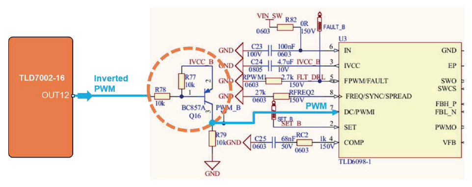
Figure 4: Shaping PWM Signal with TLD7002-16ES
Using One TLD7002-16ES Output to Cover External LED Driver PWM and Diagnostics
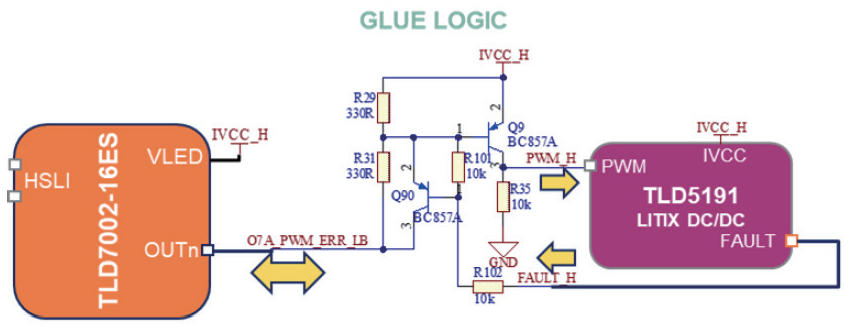
Figure 5: Logic to Provide PWM and Monitor Fault Pin
Using a single TLD7002-16ES pin and a simple bonding logic circuit, PWM functionality can be achieved while obtaining diagnostic information from the external LED driver. The main tasks of this circuit include:
-
When the TLD7002-16ES OUTn pin sinks current, it generates an inverted PWM signal to the PWM input of the external LED driver.
-
If the external LED driver fails, it generates an open-loop OL or forward voltage drop warning VFWD_WRN fault signal on the TLD7002-16ES OUTn pin.
Specific Working Principle:
The Q9 transistor effectively provides a clean (logic level HIGH/LOW) PWM signal to the TLD5191ES. If the TLD5191ES detects a fault, the FAULT_H line will be pulled low, turning on the Q90 transistor, causing the forward voltage on the OUTn pin to drop to VBE(Q9) + 0.2 V (Q90 saturation voltage). If the VFWD_WRN threshold is set to 1.25 V in the one-time programmable (OTP) memory, the reduced VFWD voltage during the external LED driver fault will generate a VFWD_WRN signal on the TLD7002-16ES OUTn pin.
It is important to note that both the VLED pin of the TLD7002-16ES and the power supply voltage for the bonding logic are connected to IVCC_H (5 V), which is provided by the TLD5191ES. This is necessary because the diagnostics of the TLD7002-16ES are based on differential voltage readings of VLED-OUTn (or VS-OUTn). Additionally, the PWM signal from the external LED driver (TLD5191ES) must operate at typical logic levels. Alternatively, the VDD pin of the TLD7002-16ES can be used as the power supply voltage for the PWM bonding logic, but it should be noted that the VDD pin can provide a maximum current of only 10 mA.
Figure 5 shows the bonding logic with the following requirements:
-
When OUTn sinks current, PWM > max PWM(H) threshold
-
When OUTn does not sink current, PWM < max PWM(L) threshold
-
Rule 1: When an error occurs, OUTn should generate VFWD (OUTn-VLED) < VFWD_WRN threshold. When calculating this requirement, assume OUTn sinks current at IOUTn(max)
-
Rule 2: When ERRN does not sink current (no error), OUTn pin should not generate VFWD (OUTn-VLED) > VFWD_WRN threshold. When calculating this requirement, assume OUTn sinks current at IOUTn(min)
Optional Rule: Ensure OUTn > OL (0.5 V) to avoid false OL detection.
Diagnostic Detection Mechanism:
-
When ERRN sinks current (error occurs), R4 is bypassed, and VFWD=VBE (Q9) + VSAT(Q90) is read by OUTn, which will generate a VFWD_WRN (low VFWD).
-
When ERRN does not sink current (no error), the voltage drop across R4 must be large enough to prevent OUTn from detecting VFWD_WRN or SLS. However, this voltage drop must not be too large to avoid triggering OL warnings.
OTP Settings
-
IOUTn = 5.6 mA. This is the minimum output current possible on the TLD7002-16 to reduce power loss.
-
VFWD_WRN = 1.25 V. This value must be greater than VBE(Q9) (at low temperature) + VSAT(Q90) when R4 is bypassed, only then will the error be detected.
Tips for Gateway Control of LED Driver Diagnostics
For instruction applications, such as BCM, to detect faults in the external LED driver channels, a TLD7002-16ES output is needed to sample the Fault (or ERR) pin of the external driver.
To utilize the diagnostic capabilities of the TLD7002-16ES, such as debounce functionality, triggering the TLD7002-16ES warning flag when the fault pin of the external LED driver is active is a convenient method. One way to achieve this is to use the fault pin of the external driver to trigger the OL warning or VFWD_WRN warning of the TLD7002-16ES. This is typically implemented through external bonding logic, as shown in Figures 9 and 10.
The OL and VFWD warning detection mechanisms are detailed in the TLD7002-16ES datasheet.
Considerations for PWM Sequence and Phase Shift on Gateway Channels
If PWM and diagnostics are executed on two different TLD7002-16 channels (see Figure 6), it is crucial to correctly assign PWM and DIAG TLD7002-16 channel numbers and understand their PWM constraints. The PWM diagnostic sequence on the gateway channel should proceed in the following order:
-
The TLD7002-16ES OUTn channel will activate the external LED driver via the PWM pin
-
The TLD7002-16ES OUTn+1 channel will sample the FAULT pin of the external LED driver
Providing PWM before the diagnostic ADC reading is beneficial to ensure that the external LED driver is activated, allowing its fault pin to be correctly sampled by the TLD7002-16. However, with appropriate debounce settings, this sequence requirement can be relaxed. To implement the above sequence, it is recommended to designate the TLD7002-16 OUTn channel as the PWM channel and the OUTn+1 channel as the diagnostic channel.
The TLD7002-16ES has a minimum PWM on-time constraint to ensure accurate diagnostic readings, as most diagnostic flags on the TLD7002-16 are based on VFWD readings. These constraints are briefly outlined here and are described in detail in the TLD7002-16 datasheet [5].
-
If phase shift is enabled: tOUTnPW > tdiag_dly + tDIAG_ON
-
If phase shift is disabled: tOUTnPW > tdiag_dly + (2+N)* tDIAG_ON
Where N equals the number of previous channels with phase shift disabled. Therefore, the gateway DIAG and PWM channels must adhere to the appropriate minimum duty cycle.
For example, in Figure 6, the gateway function is implemented on OUT1 and OUT2, while considering the following scenarios and assigning OUT0 to different LED strings:
-
The channel OUT0 before the gateway PWM channel enables phase shift, which reduces the minimum duty cycle constraints for the next two channels.
-
The gateway function PWM and DIAG channels (OUT1, OUT2) disable phase shift, which reduces the time between PWM and DIAG readings, resulting in a minimum PWM duty cycle equal to: tOUTnPW > tdiag_dly + (2+1)* tDIAG_ON
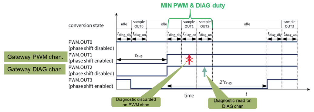
Figure 6: Timing of TLD7002-16ES Gateway Channels: PWM Generation and Diagnostic Sampling
Driving External LITIX Basic+ Linear Chips for Current Expansion
The TLD2331-3EP, as a 3-channel high-side constant current source, can be connected to the TLD7002-16ES as follows:
The three SET signals of the TLD2331-3EP are connected to the three outputs of the TLD7002-16ES, which control three IN_SET channels independently, achieving high-precision current regulation and excellent animation effects.
The ERRN pin of the TLD2331-3EP is connected to the next available output of the TLD7002-16ES for fault diagnostics.
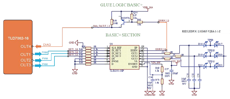
Figure 7: Driving External Linear Constant Current Source TLD2331-3EP
The connection between TLD1173-1ET and TLD7002-16ES is as follows:
One output of the TLD7002-16ES is connected to both the PWM and ERRN/DEN pins of the TLD1173-1ET. The PWM and ERRN/DEN bonding logic circuit has been detailed in previous sections.
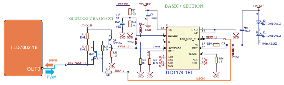
Figure 8: Driving Single-Channel Low-Side Linear Constant Current Source Chip TLD1173-1ET
Example of Gateway Application OTP Configuration
-
Set the diagnostic output group to VLED and connect the VLED pin of the TLD7002-16 to 5 V (as the PWM and ERR bonding logic is connected to 5 V)
-
If simulating the OTP of the TLD7002-16 during circuit testing or locking the SLS threshold to “locked”, otherwise the TLD7002-16 will select the default SLS threshold
-
If the PWM and ERRN bonding logic is as shown in Figure 5, set the VFWD_WRN threshold to 1.25 V. This will detect VFWD_WRN when ERRN is pulled low
-
Set the diagnostic debounce configuration to 4-6 cycles to reduce false error detection
-
Enable phase shift before the first channel of each gateway function, and disable phase shift between channels of the same gateway function
This allows for a reduction in the minimum duty cycle (see Section 7.2 of the TLD7002-16ES datasheet [5]). For example, in the circuit shown in Figure 5, by enabling phase shift on OUT0, disabling phase shift on outputs 1, 2, 3, and 4, and setting SLS to 0, the focus can be solely on the VFWD_WRN flag.
For more detailed information on OTP simulation and programming, refer to TLD7002-16 OTP Programming [3] and OTP Parameter Settings [4] application notes.
Conclusion
The TLD7002-16ES intelligent gateway chip achieves an MCU-less architecture for automotive lighting ECUs through the UART OVER CAN communication interface. This design reduces hardware complexity by 40% and wiring harness requirements by 25%, driving innovation in domain-centralized electrical design. At the same time, it better meets the dynamic configuration needs of software-defined vehicles (SDVs) for lighting systems. The single-chip integrated solution replaces traditional discrete designs, reducing BOM costs by 30%. As a cost-effective lighting control platform, the TLD7002-16ES balances functional safety, flexible scalability, and reliability upgrades, providing a solid hardware foundation for intelligent lighting systems.
This article is reprinted from Electronic Design and Chip Applications, Volume 32, April 2025. Authors: Infineon Su Xing & Fragiacomo Fabio.
Welcome to follow the Dalian Dalian Engineer Community – Dada Tong
👇👇👇


ClickRead the original text for more details!

Like
Collect
Share