
Introduction
Etching and thin film deposition are becoming the core areas of market focus.
Download for free today: 2025 Semiconductor Industry In-Depth Report
Source: Semiconductor Industry Insights
Author: Feng Ning
Recently, a financial report from Zhongwei Company reflects that the semiconductor equipment market’s focus is expanding beyond photolithography machines to include other core equipment fields such as etching and thin film deposition.
In the first three quarters of 2025, Zhongwei Company reported revenue of 8.063 billion yuan, a year-on-year increase of 46.40%. Among this, revenue from etching equipment was 6.101 billion yuan, up 38.26%; revenue from thin film equipment such as LPCVD and ALD was 403 million yuan, a staggering increase of 1332.69%.
With the development of the semiconductor industry, etching and thin film deposition are becoming the core areas of market focus.
01Latest Focus in Semiconductor Equipment
The core equipment for semiconductor manufacturing includes two main categories: front-end wafer manufacturing and back-end packaging and testing, with the highest technical barriers in front-end equipment dominating market share.
Among these, photolithography machines, etching machines, and thin film deposition equipment are the three main types of equipment. According to SEMI’s estimates, photolithography machines, etching machines, and thin film deposition equipment account for approximately 24%, 20%, and 20% of the semiconductor equipment market, respectively.
Specifically:
-
Photolithography machines act like a “projector”, transferring circuit patterns onto wafers through a light source, determining the minimum line width of chips.
-
Etching machines serve as a “sculptor”, selectively removing excess material to accurately replicate patterns.
-
Thin film deposition equipment is responsible for depositing conductive, insulating, and other layers, constructing the basic structure of chips, mainly divided into physical vapor deposition (PVD), chemical vapor deposition (CVD), and atomic layer deposition (ALD).
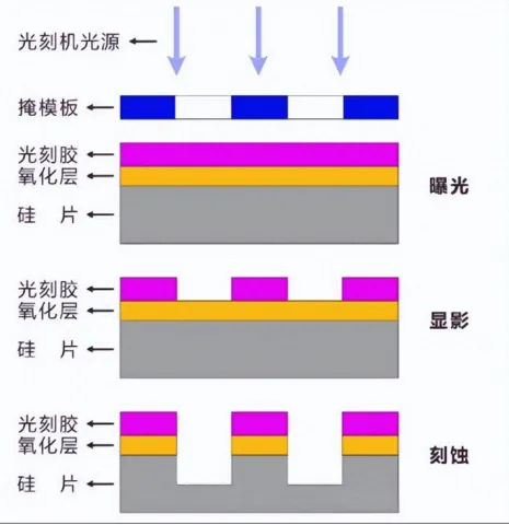
Among this series of equipment, etching and thin film deposition have become the new focus of the industry due to the inevitable logical changes brought about by the evolution of semiconductor processes to advanced nodes.
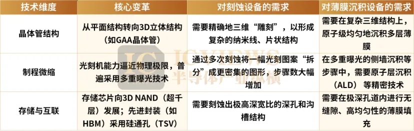
First, currently, the wavelength limit of EUV photolithography machines is 13.5nm, and the lines produced can only achieve 14nm. For chips at 10nm, 7nm, and 5nm, multiple template methods must be used to replicate the 20nm photolithography lines into two 10nm lines, and then replicate into 5nm lines.
SEMI data shows that in the chip manufacturing process, the number of photolithography steps has only increased by about 30% from the 65nm process to the 7nm process, but the number of etching steps has surged by over 300%.
At the same time, the number and complexity of thin film deposition processes are also significantly increasing. As line widths develop towards 7nm and below, multiple exposure processes are required, leading to a significant increase in the number of thin film depositions. For example, the 90nm CMOS process requires about 40 thin film deposition steps, while the 3nm FinFET process requires 100 thin film deposition steps.
Second, with the development of 3D stacked memory, 3D NAND aims to enhance storage density by vertically stacking memory cells, with the number of layers continuously increasing. Currently, mainstream products exceed 200 layers, and will further progress towards 1000 layers.DRAM also has a similar technology roadmap for 3D stacking layers. This has led to an exponential increase in demand and performance requirements for etching equipment. For instance, when increasing from 32 layers to 128 layers, the proportion of etching equipment usage increased from 35% to 48%. Additionally, the development of near-memory computing solutions has increased TSV etching demand, with etching and filling equipment accounting for nearly 70% of TSV processes, further increasing the demand for etching equipment.
At the same time, the increasing number of 3D NAND stacking layers requires strict control over the thickness of each layer, making ALD and CVD collaborative processes mainstream, which raises higher requirements for thin film deposition equipment.
Third, GAAFET is the next-generation transistor technology that will replace FinFET. Compared to FinFET, GAAFET has significantly increased etching process requirements, with 5 steps involving etching processes for FinFET, while GAAFET transistors involve 9 steps involving etching processes. According to data from IMM, the usage proportion of etching equipment in advanced processes will increase from the traditional 20% in the FinFET era to 35% under the GAA architecture, with the value of a single device increasing by 12%.
Thin film deposition equipment will need to deposit multiple layers of films uniformly at the atomic level on complex three-dimensional structures. For example: GAA nanosheet transistors require atomic-scale control of multilayer stacking (such as Si/SiGe superlattices), with the thickness deviation of dielectric films deposited by PECVD (such as gate sidewall isolation layers) controlled within ±0.5Å, and achieving conformal coverage of high aspect ratio structures (coverage rate >95%).
Therefore, the future focus of semiconductor manufacturing may shift from solely relying on photolithography machines to reduce feature sizes, to more complex and critical etching and thin film deposition processes.
02What Information Does Q3 Equipment Import Data Reveal?
According to data from the General Administration of Customs, the total import value of front-end equipment in Q3 2025 reached 10.187 billion USD, a year-on-year increase of 15.28%, and a quarter-on-quarter increase of 33.15%, setting a historical high.Changes in core equipment import data serve as a “barometer” for the domestic semiconductor capacity layout, reflecting the competitive landscape of the global semiconductor equipment industry.
Specifically:
In terms of photolithography equipment, the import quantity of “other photolithography equipment” has decreased, but the unit price of similar equipment from the Netherlands has surged to a historical high.This may indicate that the import of mid-to-low-end photolithography equipment has been reduced, focusing on introducing relatively high-end photolithography equipment to break through technical bottlenecks for advanced process expansion.
In terms of thin film deposition equipment, CVD equipment has seen both quantity and price increase, reaching a historical high, reflecting strong domestic demand for capacity expansion in advanced logic chips and high-end storage, indicating a continued high reliance on core deposition equipment like CVD. PVD equipment has achieved breakthroughs in the mid-to-low-end sector, while domestic procurement standards for high-end PVD equipment have also increased.The next focus for thin film deposition equipment will be the localization process of high-end deposition equipment such as CVD and ALD.
In terms of etching equipment, dry etching has seen significant increases in both quantity and price, which may indicate that domestic capacity expansion is shifting towards advanced processes. As chip structures evolve from 2D to 3D, the demand for high-performance dry etching equipment has surged. The import quantity and unit price of other etching and stripping equipment have both declined year-on-year, which may suggest that domestic equipment manufacturers have achieved certain results in mature process etching.
In terms of ion implantation equipment, the domestic market is currently monopolized by American Applied Materials and Axcelis, with global competition intensifying.
In terms of oxidation diffusion equipment, from the second half of 2024, the import quantity of oxidation diffusion and other thermal treatment equipment is expected to show an overall downward trend, but the import unit price continues to rise, indicating that domestic equipment has captured a certain share in the mid-to-low-end sector.
03Semiconductor Equipment: Blooming in Multiple Areas
According to the International Semiconductor Industry Association (SEMI), global spending on front-end equipment for semiconductor wafer fabs is expected to reach 110 billion USD in 2025, a year-on-year increase of about 2%. Against the backdrop of rising demand for chips at both data centers and edge computing, global spending on front-end equipment for semiconductor wafer fabs is expected to reach 129.8 billion USD in 2026, with a year-on-year growth rate of 18%.
Etching Equipment
From a technical perspective, etching processes are mainly divided into wet etching and dry etching. As semiconductor manufacturing advances to 7nm and more advanced nodes, the integration of chips continues to increase, and device structures become increasingly complex, placing unprecedented demands on the precision, selectivity, and consistency of etching processes. In this trend, dry etching has gained absolute dominance in high-end processes such as logic chips and memory chips due to its excellent technical adaptability and process control capabilities, becoming a key process driving the iteration of semiconductor technology.
In terms of the global competitive landscape, semiconductor etching equipment is mainly dominated by three manufacturers: Lam Research, Applied Materials, and Tokyo Electron, which together account for nearly 90% of the market share.
Among them, Applied Materials demonstrates strong capabilities in both CCP and ICP technology paths, with a comprehensive product line, especially leading in conductor etching and dielectric etching; Lam Research has absolute dominance in the CCP technology field, particularly in high aspect ratio etching, with its equipment becoming an indispensable core part of the 3D NAND manufacturing process.
Tokyo Electron, as the third-largest etching equipment supplier globally, shows strong competitiveness in both CCP and ICP fields, particularly in dielectric etching, keeping pace with American companies.
In contrast, domestic manufacturers such as Zhongwei Company, North Huachuang, and Yitang Semiconductor are still in the catch-up stage, with low global market share. There is still significant room for development for domestic integrated circuit manufacturers and domestic etching equipment.
Zhongwei Company is a leading company in etching equipment, with its CCP equipment covering most applications above 28 nanometers, and has made significant progress in nodes of 28 nanometers and below. In high aspect ratio etching for 3D NAND chips and front-end etching for logic chips, Zhongwei’s technology has reached some advanced nodes and is adopted by top global chip manufacturers.
However, its platform capability is relatively weak and cannot provide a full-process solution. In terms of ICP equipment, Zhongwei’s products have entered production lines for logic, DRAM, 3D NAND, and other 50 customer production lines, performing excellently in deep silicon etching for MEMS and advanced packaging, but it still needs to undergo more stringent verification cycles to enter the most complex key process steps.
North Huachuang is a platform enterprise in the semiconductor equipment field, with a leading number of semiconductor equipment categories among domestic peers, covering multiple integrated circuit production processes such as photoresist processing, etching, cleaning, thermal treatment, chemical vapor deposition, and physical vapor deposition.
In terms of technology, North Huachuang’s CCP equipment has dominated silicon etching and dielectric etching applications in 8-inch production lines, and has also been successfully applied in key non-core steps such as hard mask etching and aluminum pad etching in 12-inch production lines. Notably, its ICP equipment is developing even more robustly, with increasing market recognition.
However, in the cutting-edge applications of advanced logic chip manufacturing and high aspect ratio contact hole etching for 128-layer and above 3D NAND chips, the technical maturity, process uniformity, and stability of North Huachuang’s equipment still have room for improvement, and it has not yet entered the most advanced production lines of top global chip manufacturers.
Yitang Semiconductor was formerly the semiconductor wet equipment business unit of American Applied Materials, restructured through domestic acquisition in 2015, and has now formed three core equipment product lines: etching, thin film deposition, and rapid thermal processing. According to Gartner’s 2023 data, in the dry stripping equipment sector, Yitang ranks second globally with a market share of 34.6%; in the rapid thermal processing equipment sector, Yitang ranks second globally with a market share of 13.05%; at the same time, it is one of the few domestic companies capable of mass-producing single-wafer rapid thermal processing equipment; in the dry etching sector, its market share ranks among the top ten globally.
Thin Film Deposition Equipment
Semiconductor thin film deposition equipment is mainly divided into chemical vapor deposition (CVD), physical vapor deposition (PVD), and atomic layer deposition (ALD).
Currently, the global thin film deposition equipment market is primarily dominated by American and Japanese manufacturers such as AMAT, LAM, and TEL: in the PVD equipment sector, AMAT is in the lead with a market share of about 85%; in the CVD sector, AMAT, LAM, and TELCR3 together account for over 80%; in the ALD equipment sector, TEL and ASM together account for about 60%.
In recent years, domestic companies have continuously strengthened their technological research and development, giving rise to a number of thin film deposition equipment manufacturers such as North Huachuang, Tuojing Technology, Zhongwei Company, and Weidao Nano. However, overall, the localization strength of thin film deposition equipment is relatively weak, especially for the more technically demanding ALD equipment.
Tuojing Technology focuses on the thin film deposition equipment field, forming a series of thin film equipment products including PECVD, ALD, SACVD, HDPCVD, and Flowable CVD, which are widely used in the manufacturing of integrated circuit logic chips and storage chips, with customers including SMIC and Huahong Group.
PECVD equipment is Tuojing Technology’s core product, covering a full range of PECVD dielectric film materials, including general dielectric film materials (such as SiO2, SiN, TEOS, SiON, SiOC, FSG, BPSG, PSG, etc.) and advanced dielectric film materials (including ACHM, LoK-I, LoK-II, ADC-I, ADC-II, HTN, a-Si, etc.) have all achieved industrial application, widely used in domestic integrated circuit manufacturing lines.
In terms of ALD equipment, Tuojing Technology is a leading manufacturer in the domestic ALD equipment thin film process coverage, with ALD SiCO, SiN, AlN, and other process equipment having achieved large-scale shipments.
SACVD series products continue to maintain product competitive advantages, further expanding large-scale applications.The plasma-enhanced SAF thin film process equipment it launched has made smooth progress in client verification. By 2024, the cumulative shipment of SACVD series product reaction chambers has exceeded 100 units.
By 2024, Tuojing Technology’s HDPCVDUSG, FSG, and STI thin film process equipment have all achieved industrialization and continue to expand large-scale production, with the cumulative shipment of HDPCVD series product reaction chambers reaching 100 units. By 2024, the cumulative shipment of reaction chambers related to Flowable CVD equipment has exceeded 15 units.
Zhongwei Company had thin film equipment delivered to customers as early as 2023, mainly for CVD/HAR/ALD tungsten equipment, and TiN/TiAI/TaN ALD equipment. The Q3 2025 financial report shows that Zhongwei Company has successfully introduced multiple thin film equipment such as LPCVD and ALD developed for advanced memory devices and logic devices into the market, with equipment performance fully reaching international leading levels, and the coverage of thin film equipment continues to increase.
North Huachuang is a domestic leader in PVD, with strong scarcity, and has also made layouts in LPCVD, APCVD, and ALD fields, with products already applied in semiconductor production lines. Weidao Nano relies on ALD equipment, with applications in photovoltaics and semiconductors, and is the first domestic company to successfully apply mass-produced High-k ALD in the front-end production line of integrated circuits at the 28nm node, having a competitive advantage in the ALD field. Shengmei Shanghai started with cleaning equipment and is gradually expanding into a platform equipment company, currently launching products in cleaning, plating, Track, polishing, and thin film deposition fields.
At this year’s 106th China Electronics Fair, industry insiders told Semiconductor Industry Insights that from 2010 to 2024, the compound annual growth rate of domestic semiconductor equipment sales reached 30.2%, significantly higher than the global market during the same period. The growth shows obvious phased characteristics: In 2017-2018, due to the concentration of leading wafer manufacturers starting the construction of 12-inch production lines, equipment procurement demand was concentratedly released; in 2023-2024, benefiting from the expansion of mature processes (28nm and above) and the landing of specialty processes (such as SiC, GaN), the growth trend continues to solidify, and it is expected that by the end of 2024, it will still maintain a year-on-year growth rate of 25%-30%.
However, it should be noted that although the localization progress of etching and thin film deposition equipment has accelerated, the key component links have become one of the bottlenecks for self-control. Currently, the supply chain for general standard parts of these two types of equipment is highly dependent on imports: Japanese companies (such as NSK, Fujikin) occupy most of the market share, mainly providing high-precision transmission components and special gas control components; European suppliers (such as Pfeiffer, Leybold) account for more than half of the vacuum system field. American component companies still control part of the core customized component market.
However, this restrictive pattern is now facing a dual breakthrough opportunity driven by policy guidance and market forces: the National Integrated Circuit Industry Investment Fund Phase III (Big Fund Phase III), with a total scale of 344 billion yuan, has clearly listed upstream key components as one of the core investment directions. Subsequent measures to reduce dependence on overseas supply chains will lay a solid foundation for the localization of etching and thin film deposition equipment.
Recommended Reading:1. Detailed Explanation of the Photolithography Machine Industry Chain2. Overview of Computing Power-Related Industry Chains3. Comprehensive Overview of the Automotive Industry Chain in A-shares4. Analysis of the Domestic Collection Industry5. Ranking of Chinese Unicorn Enterprises
——END——
[PS: Click for details to view content]

Click the WeChat mini program 👉: “Report Search”; Download various industry research reports in PDF and Word, visual data, and learning materials. Provides research reports, market research reports, industry reports, industry research reports, survey reports, market survey reports…