 In-depth exploration of diamond’s applications in power electronicsWide bandgap semiconductors are considered the next frontier in the field of power electronics. These materials include gallium oxide, aluminum nitride, and diamond, which have significant theoretical advantages over wide bandgap devices made from silicon carbide or gallium nitride. This article will discuss some of these advantages and the practical challenges encountered during implementation, introduce recent research findings on diamond devices, and showcasePatrick Le Fevre, PRBX’s Director of Marketing Communications, in the latest white paper titled “Will Diamond Become the Ultimate Semiconductor?”(For the original white paper, please see the end of the article)highlighted application scenarios.Characteristics of Diamond SemiconductorsTable 1 compares some basic material properties of silicon, silicon carbide, gallium nitride, and diamond.
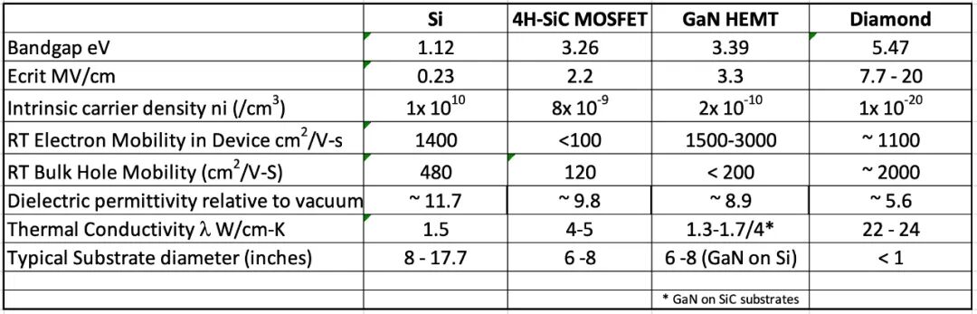 Table 1: Comparison of Some Material PropertiesDiamond’s higher bandgap width results in a much higher critical electric field and breakdown strength. Its high bulk carrier mobility leads to lower conduction losses and higher current density advantages, while its low dielectric constant helps achieve low power consumption and miniaturized designs in high-frequency scenarios.Diamond has the highest thermal conductivity of all known materials. This means lower thermal resistance, allowing for higher power density at a given junction temperature rise, and lower thermomechanical stress,which also provides application motivation for its use as a heat dissipation substrate material.Other Unmentioned AdvantagesIn addition to the properties listed in Table 1, diamond also has the following advantages: Electrons on hydrogen-terminated surfaces can exchange locally with the valence band, promoting the formation of 2D hole gases (2DHG); high radiation resistance gives it a core competitive edge in high-radiation special scenarios (examples will be provided below); leveraging the plasma oscillation principle of 2DHG, diamond performs outstandingly in the sub-THz to THz frequency range, with its high hole momentum relaxation time becoming a key competitive advantage.Technical Bottlenecks and Challenges
- Substrate Preparation Challenges:The main bottleneck in the development of diamond electronic devices is the preparation of high-quality, large-size substrates. The HPHT process can synthesize diamond crystals at temperatures above 2000°C and pressures above 10 GPa, suitable for producing small-sized (approximately 1 cm²) high-quality type IIa substrates; while the more cost-effective CVD method is more suitable for electronic applications, capable of producing larger substrates (typically with diameters <2-3 inches). The commonly used Ib-type substrates containing isolated nitrogen atoms have a defect density of about 10⁵/cm², while silicon carbide substrates typically have a defect density of about 10²/cm². Homogeneous epitaxial CVD uses HPHT seed crystals as the substrate, while heterogeneous epitaxial CVD uses heterogeneous substrates such as iridium-coated silicon or cubic silicon carbide, which can achieve larger sizes but will increase stress and defect density.
- Doping Technology Challenges:Boron can be used to create p-type diamond, with doping typically occurring during the CVD growth process. Low doping concentrations are easy to achieve, but high concentrations and thick doping can lead to decreased crystallinity, making it more difficult. The acceptor energy level of boron is 0.37 eV from the valence band, which is not completely ionized at room temperature, but higher net hole concentrations can be obtained at temperatures above 500K with the same doping concentration. Nitrogen and phosphorus can be used as n-type dopants, but their energy levels are deeper, making n-type doping difficult.
- Hydrogen Termination and Device Characteristics:Hydrogen termination can form 2DHG through a surface transfer doping mechanism, with achieved carrier mobilities of about 300 cm²/(V·s), although lower than that of bulk material, but temperature-independent. The net carrier concentration of bulk diamond increases with temperature, leading to a negative temperature coefficient characteristic of the conduction resistance in bulk conductive diamond devices, which makes diamond devices significantly more efficient in power conversion at high temperatures (400K/450K) compared to wide bandgap devices, but the negative temperature coefficient can lead to current crowding risks in parallel devices, potentially causing thermal runaway. Current research is mainly focused on unipolar devices, while the high built-in voltage (4.9V) and short carrier lifetime of p-n junctions limit the application of bipolar devices in high-temperature, low-frequency scenarios.
Representative Device AchievementsSignificant device achievements published include:p-type lateral Schottky barrier diodes (SBD) using aluminum oxide field plates, with breakdown voltages reaching 4,612 V; vertical depletion-mode p-MOSFETs based on 2DHG and using Al₂O₃ gate dielectric, achieving conduction currents exceeding 1 amp; and enhanced p-MOSFETs based on 2DHG with UV ozone-treated modified H-terminated surfaces.Donato et al.’s theoretical quality factor analysis indicates that for a 1,700 V vertical unipolar power FET, under conditions of 425 K/450 K, 20 kHz switching frequency, 1,200 V, and 50 A, the size of diamond devices will be nearly 10 times smaller, with power losses reduced by a factor of 3. However, the smaller effective size leads to much higher power density in diamond devices, placing greater demands on thermal management systems.Reliability and Integration ChallengesReliability of diamond devices under the harsh environments corresponding to their theoretical advantages still needs to be verified, which may require the establishment of new testing standards and technical methods. Although the advantages of diamond become increasingly significant at higher junction temperatures, theoretically simplifying heat dissipation design, its integration with other devices (such as n-type wide bandgap devices used to complement p-type diamond devices and gate drivers) faces thermal engineering compatibility issues, potentially requiring customized packaging solutions.Application Cases1. Nuclear Environment Electronic Devices:In March 2011, the Fukushima Daiichi Nuclear Power Plant experienced a severe core meltdown due to a tsunami. The extreme radiation environment posed stringent requirements on electronic devices used for debris cleanup and data collection. The Japanese startup Ookuma Diamond Device, originating from a collaboration between the Japan Atomic Energy Agency, Hokkaido University, the National Institute of Advanced Industrial Science and Technology, and the High Energy Accelerator Research Organization, underwent ten years of research and development, establishing the world’s only fully vertically integrated production base in 2022. Its laboratory device yield reached 90%, successfully demonstrating a diamond MOSFET differential amplifier prototype circuit that can operate at 300°C.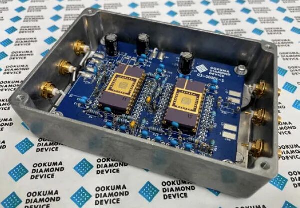 Diamond MOSFET differential amplifier prototype (Source: Ookuma Diamond Device)2. Aviation Power Conversion:The French startup DIAMFAB, spun off from the French National Center for Scientific Research (CNRS) and the Neel Institute, focuses on diamond epitaxial growth and device development, currently offering p-type doped wafers suitable for SBD or FET. The company, in collaboration with the Neel Institute and the Plasma and Energy Conversion Laboratory, successfully developed a body forked p-JFET device with a total gate width of 14.7 mm, achieving conduction currents exceeding 50 mA. This project is part of the European “High-Altitude Diamond Converter and Arc Fault Detection” program, aimed at providing power conversion and management solutions for the next generation of all-electric aircraft.3. Complementary Inverters:Traditional inverters use two n-channel devices and require dead time between device turn-off/on to prevent bridge arm shoot-through, but dead time can lead to increased conduction losses in the freewheeling diodes and output distortion, limiting switching frequency improvements. Complementary inverters composed of p-channel and n-channel devices can simplify gate drive design and minimize dead time. However, p-channel devices made from silicon carbide and gallium nitride face issues of low mobility and poor performance. Recent research by Kawai et al. indicates that complementary inverters composed of diamond p-FETs and n-type silicon carbide/gallium nitride FETs can operate stably at 100 kHz, effectively addressing this pain point.For the complete original document of PRBX’s “Will Diamond Become the Ultimate Semiconductor?” white paperplease scan the QR code to add the SIW service team
This translation is for reference only; please refer to the original English document for accurate information.
The link to the original English document is as follows,or click to read the original text.
https://www.powerelectronicsnews.com/a-deeper-dive-into-diamond-in-power-electronics/Disclaimer:All content is obtained through public and legal channels, and the copyright belongs to the original writing/publishing organization. If there are any copyright or other issues, please contact us.Content is recommended reading for reference and learning; if there are doubts about the content, please contact the original writing/publishing organization.
AboutSIW
Focusing on the ecological service platform in the vertical field of semiconductors, adhering to the“Collaboration, Innovation, Win-Win”values, implementing the concept of“Breaking technical barriers through ecological collaboration and reshaping the industry landscape through vertical innovation,” the vision is to become an indispensable strategic partner behind the semiconductor industry.
As a builder of the industry ecosystem, we provide comprehensive services covering ecological resource integration, strategic frontier research, and industry marketing training. By creating a series of self-operated brand columns, we promote in-depth communication within the industry, supporting enterprises in transforming technological competitiveness into market influence through professional brand operation and communication.
Relying on a core team with nearly thirty years of industry experience, we have established offices in Taiwan, Shanghai, and Wuhan, with three locations working together to radiate the Asia-Pacific and global markets, possessing the resource integration capability covering the entire semiconductor industry chain. Currently, we have served numerous industry-leading enterprises and institutions, assisting Chinese semiconductor companies in achieving domestic substitution and global leapfrogging through ecological full-cycle solutions.