Hello, dear readers.Recently, a cement plant underwent technical transformation and production line upgrades. The foreign DCS control system that had been running in one of its lime kilns for over 20 years began to be gradually replaced due to outdated technology, missing parts, and the inability to configure AI tools. The system replacing the DCS is a special controller based on the VPX architecture, which is relatively rare in domestic industrial control systems. The author has conducted reverse architecture speculation and analysis for your review.First, let me report on what the VPX architecture is:VPX refers to the Vita46 protocol, which consists of a series of sub-specifications including bus architecture, mechanical structure, and electrical signals, forming a modular-level specification that is a high-speed serial bus standard.
The technologies required in VPX include:● 3U and 6U formats● New 7-row high-speed connectors with a rated speed of up to 6.25 Gbit/s● PMC, FMC (VITA 57), and XMC (VITA 42) mezzanines● Hybrid backplanes that accommodate VME64, VME320 VXS, and VPX boardsFor finer details, please allow me to refrain from further explanation here; Doubao provides a more detailed explanation.
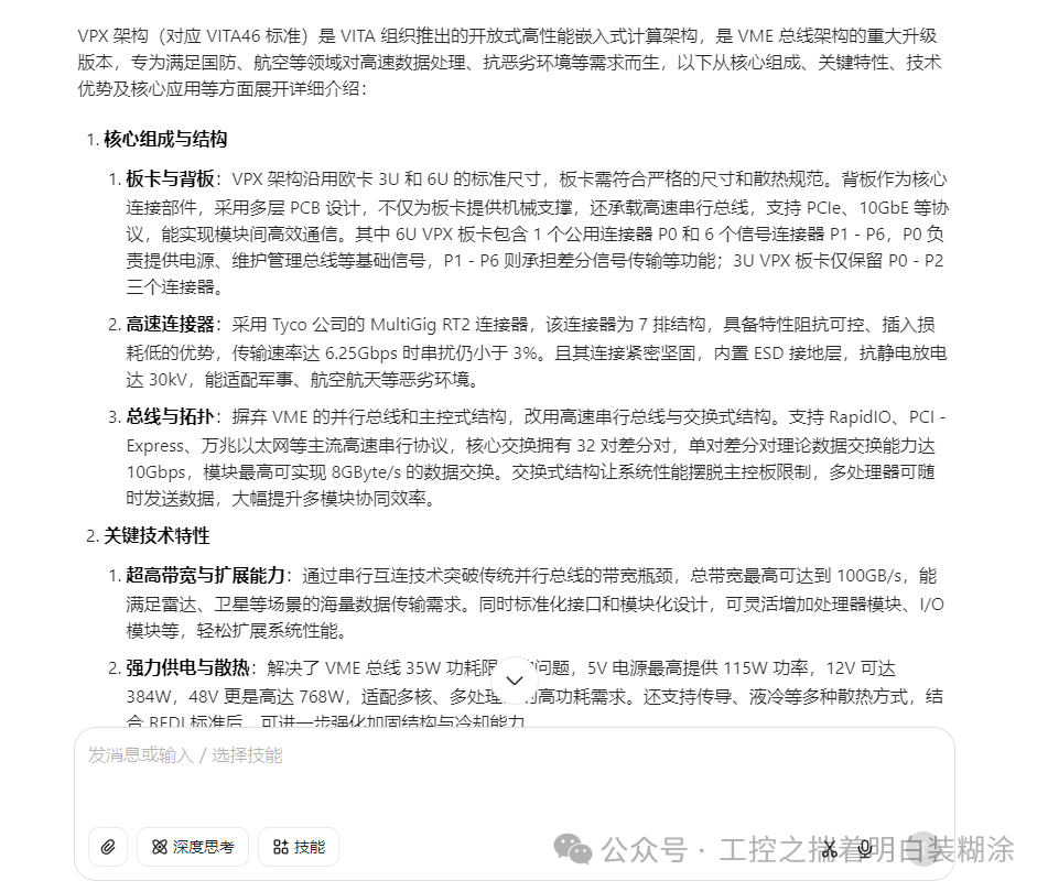
The overall architecture diagram is shown below.
The architecture diagram was drawn by the author using Visio based on the architectural design. It is relatively rough; at the bottom is the VPX backplane communication, which has multiple CPU main control boards. The main control boards are designed with FPGA, and each main control board is configured with relevant peripheral interfaces. Among them, multiple main control boards share an external Ethernet connection to communicate with the monitoring system, MES, etc.;
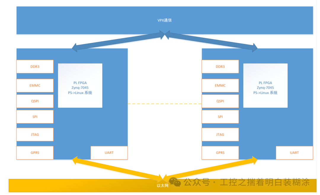
The architecture diagram is not particularly difficult. It includes a GPRS module for remote data monitoring (especially for cross-border data monitoring) and upgrades. The data plan is purchased from a certain operator, and after verification, this system can be directly applied to similar industrial scenarios abroad.
Power supply circuit:
The power supply chip is crucial. As you all know, the TPS series power supply chips from TI in the USA are almost famous in the industry, and many domestic inverter manufacturers use them; they are indeed sturdy and durable. However, there are many other options in the industry;
The author chose the LTM4644, which is also a good power supply chip from ADI. More importantly, many Xilinx development boards recommend using this chip. The external +12V can be converted to +3.3V, 1.8V, 1.2V, etc.; it has also passed the test in industrial application scenarios.
Additionally, the author uses Micron’s DDR3 for storage (although DDR prices have skyrocketed, it must be used; later, we will see if there are other alternatives);
OK, let’s talk about the CPU chip, which is the Xilinx Zynq-7000 series new xc7z045, a heterogeneous chip with ARM + FPGA, featuring a dual-core ARM Cortex-A9 + FPGA. Both the PS side (ARM + Linux) and the PL side (FPGA) are configured with DDR3 chips;
This chip has been around for many years and is quite mature, with strong computing power and ample resources, having been tested in the industrial control market.
Recently, DDR memory chip prices have risen sharply; sigh, once again, I complain about some unscrupulous manufacturers hoarding.
| Processor | 7Z045 |
| Clock Speed | 800MHz |
| Level 1 Cache | 32KB |
| Level 2 Cache | 512KB |
| Peripherals | 2*SPI; 2*UART; 2*I2C; 2*CAN |
| Lookup Tables (LUTs) | 218600 |
| FIFO | 437200 |
| BRAM | 2.4MB |
| Logic Units | 350K |
Let me first introduce the hardware design of the power supply module:
According to the RM manual of the Xilinx Zynq 7Z045 chip, the working voltages of multiple BANKs are different, so based on the LTM4644 power supply chip, specific selections are made;
The chip is powered externally by 12V, which at least ensures that the PS side operates normally;
The circuit diagram of the power supply chip is shown below;
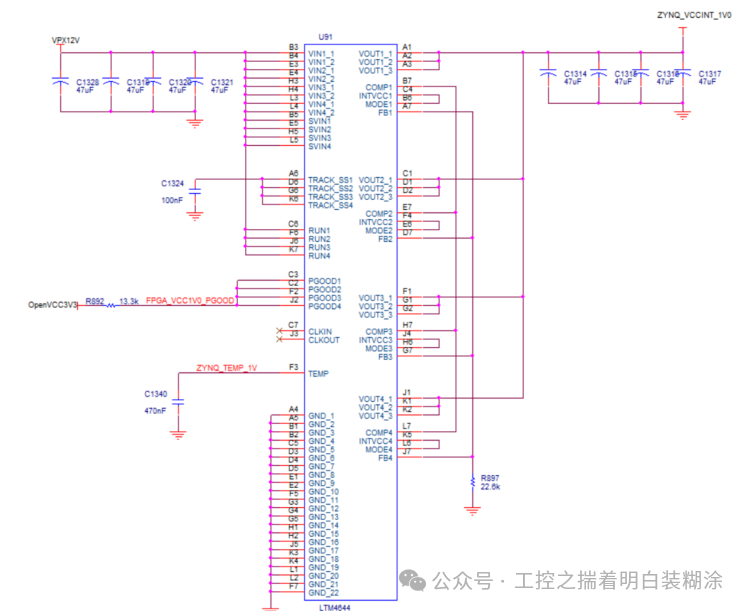
There is not much to say about the power supply chip; it converts 12V to 1.8V and 3.3V, then uses LDO for voltage regulation, supplying 1.5V to DDR and 1V to the Xilinx Zynq chip;
Of course, it also suppresses high-frequency noise and spikes on the power lines, absorbs static electric pulses, and ensures the stability of the power supply voltage VCC for the Zynq xc7z045 main chip. By utilizing the capacitor’s “decoupling” characteristics and energy storage properties, multiple decoupling capacitors were added under the pins during the design process to form a voltage filtering circuit; I won’t elaborate further here, and the circuit diagram is as follows;

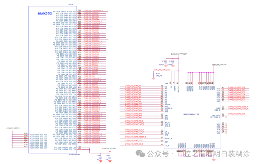
Additionally, the DDR3 circuit diagram is shown below: I personally believe this is the least technically challenging part; just directly copy the official design circuit; however, it is important to pay attention to equal length design during layout.
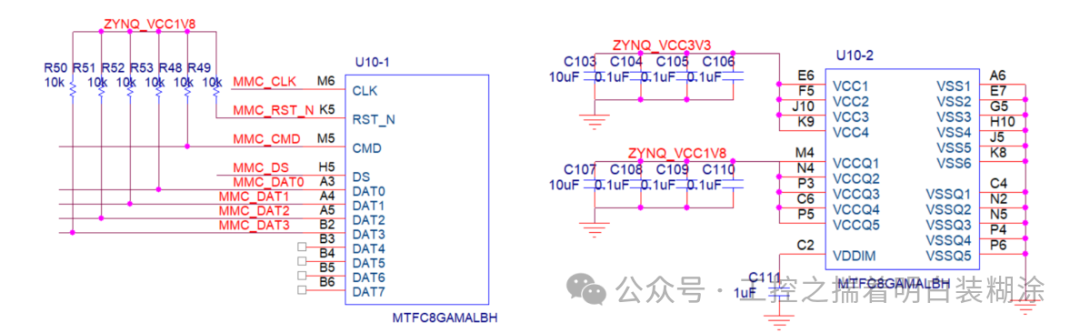
The EMMC circuit design is shown in the following diagram:
The EMMC uses the MTFC8GAMALBH chip, with a storage capacity of 8GB and a clock speed of 200MMHz, operating at a voltage of 2.7~3.6V:
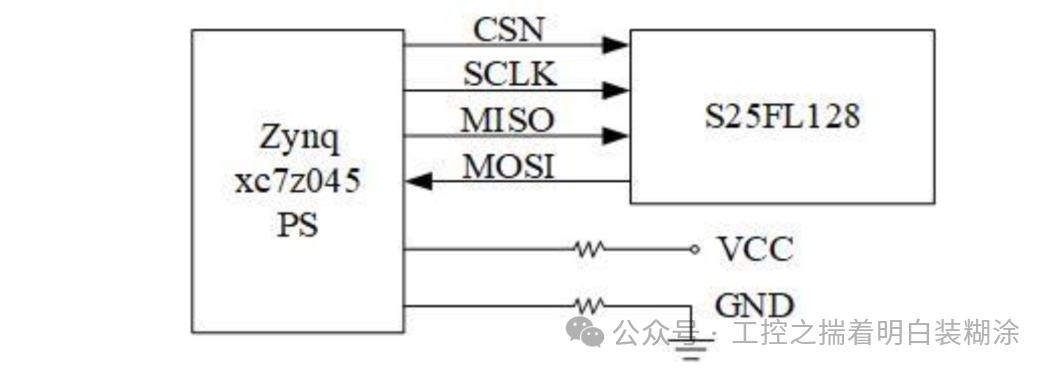
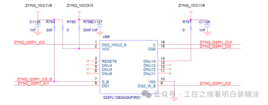
Additionally, the QSPI storage circuit is shown in the following diagram, using the SPI interface, connected to the S25FL128SAGMFIR01 chip with 128Mbit (small b) storage.
The JTAG, UART, and GPRS circuits are relatively mature, with the GPRS module being independent and capable of direct communication via SPI; I won’t elaborate further here;
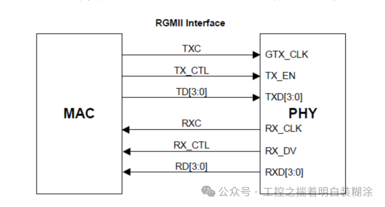
The Ethernet circuit generally has a chip with a built-in MAC, and then an external PHY chip converts the MAC’s digital signal into an analog signal, which is then transmitted to the transceiver, with an external crystal head interface:
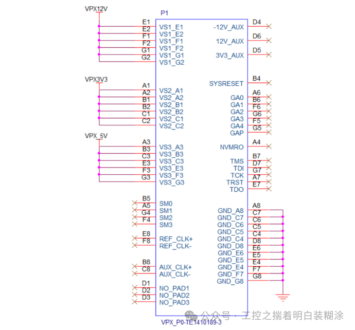
The circuit design of VPX, including connectors, is also quite particular.
Due to the high-speed communication characteristics of VPX and the high stability requirements of industrial control systems, it is recommended to use foreign connector structures;
Overall, the introduction to the circuit design is as above. PCB design is also very important. Frankly speaking, PCB design needs to comprehensively consider factors such as signal consistency, power stability and integrity, signal crosstalk, and electromagnetic compatibility (EMC). Layout engineers must reasonably plan component layout and design stacking structures based on requirements.
Many leading domestic automation manufacturers and some military enterprises have very high standards for layout, establishing review standards to achieve optimal results.
Due to the numerous signal lines in this control system, including the processing and wiring of high-speed signals, the PCB board adopts a design with more than 10 layers, including at least 2 power layers, 5 ground layers, and 8 signal layers.
During PCB layout, the principle of “first large then small, first difficult then easy” should be followed. The core board should be designed first, ideally grouping core components and high-frequency signal modules together; additionally, analog signals should be separated from digital signals, and high-frequency signals from low-frequency signals, which is basic practice. A symmetrical layout should be adopted for aesthetic purposes; heating devices such as MOSFETs (if there are no high-power devices, it’s fine) should be equipped with heat sinks for cooling. During PCB wiring, right angles and sharp angles can cause changes in line width (I had design issues when I was studying…), leading to impedance discontinuity; 45° angles should be used for turns; delay should be adjusted, coupling minimized, and system timing design requirements met; circular wiring can easily form a loop antenna, causing radiation interference; signal lines should maintain sufficient spacing to reduce inter-line crosstalk. Increasing the copper area for power and ground enhances heat dissipation capability.
All of the above are experiences; friends who want to learn hardware should study more to at least avoid being misled…
Other aspects such as FLASH and DDR, and the equal length design of network chips should be given more attention later; otherwise, debugging can become problematic and troubleshooting inconvenient.
Some readers may wonder why not switch to the latest PLC or DCS? Although using FPGA on-site is not as versatile as PLC, FPGA offers good flexibility, which is very helpful for future function expansion and production line scaling. It is said that this product will also be applied in a certain industrial control scenario abroad.
Some motors in the cement plant still use traditional DC motors, controlled by hard wiring. Due to the high difficulty and cost of replacement, they were not changed to AC variable frequency this time. The VPX controller connects directly to the existing wiring through its integrated IO interfaces, which also requires high hardware protection capabilities.
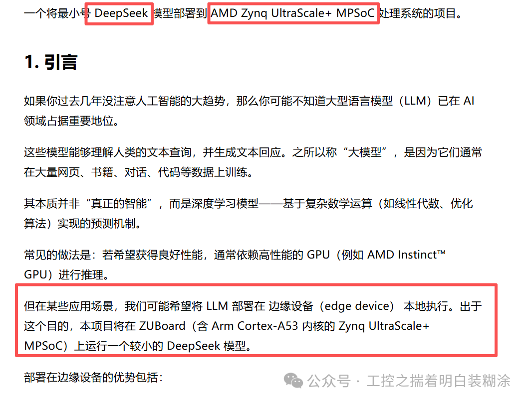
I originally wanted to discuss the AI architecture at the FPGA level in detail. The PS side of the heterogeneous FPGA chip can run Linux, allowing for the porting of some simple models. However, the main AI large models are still on the monitoring system’s server side. Here, I would like to quote a description from a certain homepage, as I believe they express it better than I do. I hope everyone can study it seriously.
Deploying the DeepSeek model locally on ZYNQ
Fragmented Thoughts, WeChat Official Account: OpenFPGA Edge AI New Play: Deploying the DeepSeek Model Locally on ZYNQ
Xilinx’s official website has reference circuit diagrams for FPGA development boards, which everyone can download if needed.
Thank you all for your understanding and support as I organize this information.