Printed Circuit Board
Comprehensive Design
The comprehensive design of a Printed Circuit Board (PCB) is a complex process that involves multiple fields such as electronic engineering, materials science, thermodynamics, and signal integrity.
1. Preliminary Design Preparation
1. Requirement Analysis
Functional Requirements: Division of circuit functional modules (power supply, control, communication, etc.)
Performance Indicators: Operating frequency, power density, EMC requirements
Mechanical Constraints: Dimensions, installation methods, connector positions
Environmental Requirements: Operating temperature range, dust and water resistance levels
2. Schematic Design
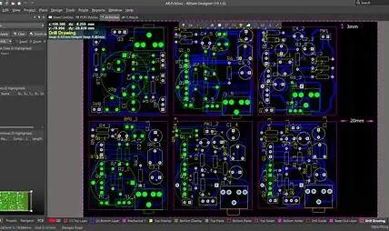
Using EDA tools (such as Altium Designer, KiCad, Cadence, etc.)
Establish component libraries: Synchronize verification of symbol libraries and package libraries
Generate netlist: Ensure electrical connection correctness
2. Core Design Phase
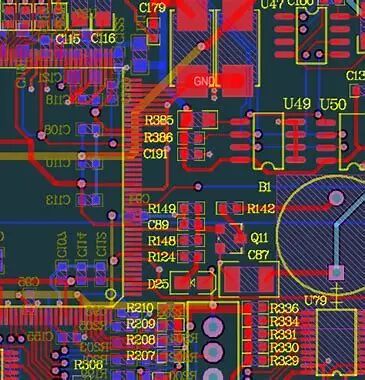
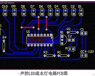
1.Layout Design
Functional zoning principles
Prioritize layout of key components: CPU, high-frequency devices, power devices
Thermal planning: Layout of heat-generating components and heat dissipation channels
Interface component positioning: Comply with mechanical structure requirements
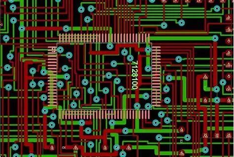
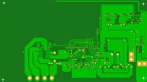
2.Routing Design
Signal integrity control:
Impedance matching (microstrip line/stripline calculation)
Equal length routing (high-speed differential pairs, DDR, etc.)
3W principle (line spacing ≥ 3 times line width)
Power integrity:
Power plane segmentation
Decoupling capacitor layout (distributed by frequency band)
Electromagnetic compatibility design:
Sensitive signal shielding
Minimize ground loop
Filter circuit layout
3.Stack-up Design
Typical 4-layer board structure:
Top Layer
GND Plane
Power Plane
Bottom Layer
High-speed board recommendations:
Signal layers adjacent to reference planes
Symmetrical stack-up structure to control warpage
3. Design Verification and Optimization
1.Design Rule Check (DRC)
Line width/line spacing verification
Hole aspect ratio check
Solder mask bridge check
2.Signal Integrity Simulation
Using tools such as HyperLynx/Sigrity
Key signal eye diagram analysis
Cross-talk simulation
3.Thermal Simulation Analysis
Identify thermal hotspot areas
Evaluate the effectiveness of heat dissipation solutions
4. Manufacturing Output Preparation
1.Production File Generation
Gerber files (RS274X format)
Drilling files (Excellon format)
Assembly drawings (including component coordinate files)
2.Process Requirements Specification
Surface treatment options:
Conventional: HASL (Hot Air Solder Leveling)
High density: ENIG (Electroless Nickel Immersion Gold)
Special processes:
Blind and buried vias
Impedance control tolerance
5. Design for Manufacturability (DFM)
1.Component spacing control:
SMD component spacing ≥ 0.3mm
5mm no-layout zone around connectors
2.Pad Design:
Solder mask opening compensation
Test point design (diameter ≥ 0.8mm)
3.Edge Treatment:
V-cut or stamp hole design
Process edge width ≥ 5mm
6. Debugging and Verification
1.First Board Inspection:
AOI (Automated Optical Inspection)
ICT (In-Circuit Testing)
2.Functional Verification:
Power system testing (ripple/noise)
Signal quality testing (rise time/overshoot)
EMC pre-testing (radiated emissions/immunity)
7. Design Iteration Optimization
1.Issue tracing mechanism
2.Version control management
3.Accumulation of design experience
8. Advanced Design Techniques
1.Key points for high-speed design
Back drilling technology (elimination of Stub)
Serpentine routing for length compensation
Via optimization (handling of Via stub)
2.RF Circuit Design
Co-planar waveguide structure
Antenna feed point impedance matching
Shielding cavity design
3.Rigid-flex board design
Bending radius control
Stress relief in transition zones
Common Design Standards
1. IPC Standards:
IPC2221 (General Standard)
IPC7351 (Package Design)
IPC6012 (Rigid Board Specification)
2.National Standards:
GB/T4588 series
Recommended Toolchain
Schematic Design:OrCAD, PADS Logic
PCB Design:Allegro, Altium Designer
Simulation Tools:ANSYS SIwave, Keysight ADS
Version Management:Git + Altium 365
Design Quality Assessment Metrics
1.First Pass Yield (FPY)
2.Mean Time Between Failures (MTBF)
3.Wiring density per unit area
4.EMC certification pass rate
A successful PCB design requires a balance of electrical performance, manufacturability, and cost-effectiveness. It is recommended to adopt a modular design approach, establish standardized design specifications, and validate key designs through simulation in advance. With the advancement of technology, it is advisable to focus on:
HDI (High-Density Interconnect) technology
Embedded component technology
3D printing PCB technology
AI-assisted routing technology
Remember to conduct at least 3 design reviews before formal mass production and reserve 10-15% of the budget for design iteration optimization.
END