According to IDC data, global shipments of wearable devices reached 138.4 million units in Q3 2021, a year-on-year increase of 9.9%. In the domestic market, shipments reached 35.28 million units, up 5.0%. It is expected that global shipments of smart wearable devices will reach 632 million units by 2024.
In the small-sized wearable devices, power management has always been a key focus of the industry and is crucial for enhancing user experience. As the functions of wearable devices continue to expand, their system energy consumption has also significantly increased. Using an efficient PMIC can effectively improve power conversion efficiency, reduce system power consumption, maximize performance per watt, and extend battery life.
Qorvo’s Low-Power PMIC for Medical Wearables
When it comes to wearable PMICs, some may be surprised to hear about Qorvo. Many associate Qorvo with providing wireless RF solutions, being a leader in communication base stations, mobile RF chips, and IoT RF chips. When did Qorvo enter the PMIC field? In fact, as early as 2019, Qorvo acquired Active-Semi, a company focused on power management and motor driver chip design and R&D.
Active-Semi has a wealth of experience in the PMIC field, and its previously launched PMICs have received recognition from many manufacturers, capturing nearly 50% of the market share in the action camera niche. With the rise of the wearable device market, there is a strong demand for PMICs that can be applied to small devices. Qorvo has leveraged Active-Semi’s advantages in the PMIC field to launch the ACT81460 PMIC suitable for wearable devices.
ACT81460 is a PMIC released by Qorvo for small battery-powered systems. This chip integrates a linear charging function, with a static current of 6μA, and an extremely low standby current that enhances battery life, especially for devices that remain in standby mode for extended periods or operate with low power. To further improve battery-powered device endurance, Qorvo has also designed a low-power operating mode for it, which allows the ACT81460 to configure the number of regulators to be turned on or off according to actual needs, thereby maximizing battery efficiency.
ACT81460 supports voltage inputs from 4V to 5V. The chip also integrates three low-dropout regulators, three load switches, four configurable GPIOs, and four efficient DC/DC converters, including two buck converters, one buck-boost converter, and one boost converter that supports up to 20V. The output values of each DC/DC converter can be configured via I2C according to actual application needs. Due to the high efficiency of the DC/DC converters, this PMIC can fully utilize battery voltage down to 2.7V. The chip uses a WLCSP package with dimensions of 3.3*3.3mm, meeting the miniaturization requirements of wearable devices.
Maxim’s Multi-Output PMIC with 50% Size Reduction
In the wearable field, Maxim has launched several products to date, including the max20310, which is a PMIC with ultra-low static current previously released by Maxim. This chip consists of two single-inductor and two low-dropout regulators along with other power management components.
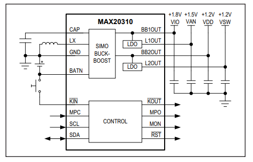
Circuit Topology Image Source: Maxim
The max20310 adopts an innovative single-inductor multi-output architecture, capable of providing two programmable voltage output channels while using a single inductor, thereby minimizing chip size and enhancing design flexibility for end products. This design also reduces the static current of each output to the lowest level, achieving over a 40% reduction in standby static current compared to traditional discrete design solutions.
Additionally, the chip supports operation at a minimum battery voltage of 0.7V, maximizing battery utilization, and supports output voltages above or below the battery capacity voltage. The two integrated low-dropout linear regulators with programmable capabilities can also act as power switches in the system circuit, disconnecting peripheral devices to reduce unnecessary energy loss. A multiplexer is also integrated, which can be used to monitor the power input/output status of each function of the chip.
In terms of specific parameters, the battery input range of the max20310 is between 0.7V and 2.0V, and the output voltage ranges from 0.9V to 4.05V, allowing configuration based on actual needs. The maximum total input power supported by the chip is 250mW, achieving an efficiency of 84% at an output power of 1.8V/10mA. The chip uses a WLP package with dimensions of 1.63*1.63mm, reducing size by nearly 50% compared to similar products. Overall, this chip meets the application requirements for wearable devices in terms of low power consumption and small size.
In wearable devices, small-sized PMICs contribute to the miniaturization design of terminal applications, improving layout flexibility. They also reserve valuable space for the realization of more functions. Low static current can more effectively extend device battery life, enhancing user experience. As wearable devices develop rapidly, it is believed that even lower power consumption and smaller size products will soon enter the market for terminal manufacturers to choose from.

Disclaimer: This article is original from Electronic Enthusiasts. Please indicate the source above when reprinting. For group communication, please add WeChat elecfans999. For submission inquiries, please email [email protected].
More Hot Articles
-
After AMD’s Acquisition of Xilinx, Is the Fate of Domestic FPGA Manufacturers Already Determined?
-
The Chip Landscape of Automotive Giants: Frenzied Exploration of the Next High Ground
-
The “East Data West Calculation” Project Fully Launched: Major Opportunities in Servers, Power Supplies, Photovoltaics, and Energy Storage
-
Samsung Strikes Threat, Micron and Western Digital Price Hikes: When Will Domestic Storage Chips Hold Their Ground?
-
28nm Carbon Chips Equivalent to 7nm Silicon Chips?! A Cold Reflection on Domestic Carbon-Based Chip Fever