Power management converts different power inputs into output voltages that meet system requirements through specific circuit topologies. The power supply directly affects system performance, and the key component that determines power supply performance is the Power Management Integrated Circuit (PMIC). It is essential to understand the guidelines for selecting PMICs.
Understand the Power Usage Environment
To select the appropriate power management components, one must first understand the application environment conditions, such as the system’s input and output parameters. These considerations include: Is the power input AC or DC? If it is direct power, is it powered by USB or a battery? Is the input voltage higher or lower than the required output voltage? What is the required load current? Is the load sensitive to noise, or does it require constant current (such as in LED applications), or does it have varying current? What is the installation space? Achieving higher power in a smaller space.
Different applications have their specific needs and require corresponding power conversion schemes and matching power management ICs. Common ICs include Low Dropout Regulators (LDO) and DC/DC switching converters. Among these, DC/DC switching converters include three types: Buck converters, Boost converters, and Buck-Boost converters.
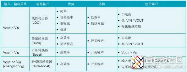
In circuit design, the first consideration is the voltage difference between input and output (VIN – VOUT). Next, based on the specific requirements of the application, such as efficiency, thermal limitations, noise, complexity, and cost, select the most suitable power management IC.
When VOUT is Less Than VIN When VOUT is less than VIN, the required output current and the VIN/VOUT ratio are important factors in choosing between LDO or Buck. (1) Choose LDO for Low VIN/VOUT Applications LDO linear regulators control the conduction of the conducting element in a linear manner to adjust the output voltage, providing accurate and noise-free output voltage, and can quickly respond to changes in load at the output. Therefore, they are very suitable for applications requiring low noise, low current, and low VIN/VOUT. When selecting an LDO, consider the range of input and output voltages, the current size of the LDO, and the thermal capability of the package. The voltage difference of LDO refers to the minimum voltage between VIN and VOUT within the adjustable range. In micro-power applications, where a single battery may power the device for many years, the LDO’s quiescent current (IQ) must be low to reduce unnecessary battery consumption; such applications require special LDOs with low quiescent current (IQ). However, linear regulation means that the voltage difference between input and output multiplied by the average load current is the power consumed by the linear regulator’s conducting element. A high VIN/VOUT ratio and high load current can lead to excessive power loss. High power-consuming LDOs require larger package sizes, increasing costs, PCB space, and thermal dissipation.
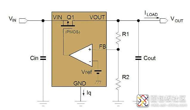
Basic Circuit Diagram of LDO
When the power consumption of the LDO exceeds approximately 0.8W, it is wiser to switch to a Buck converter as an alternative. (2) Choose Buck Converter for High VIN/VOUT Buck converters are a type of switching step-down converter that can provide high efficiency and high flexibility under high VIN/VOUT ratios and high load currents. Due to their wide application, Buck converters are also known as step-down regulators or DC-DC step-down switching regulators, essentially referring to the same product. Most Buck converters include an internal high-side MOSFET and a low-side MOSFET as a synchronous rectifier, controlling the alternation of both through an internal duty cycle control circuit to adjust the average output voltage. Noise caused by switching can be filtered by external LC filters.
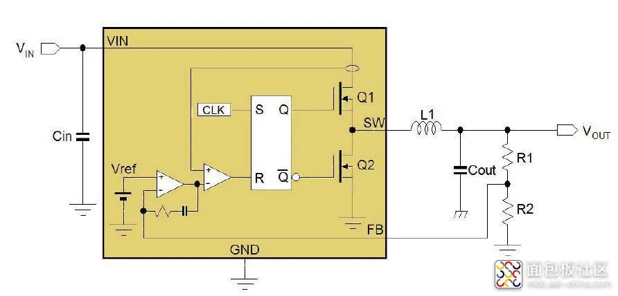
Basic Circuit Diagram of Buck Converter
Since the two MOSFETs switch alternately (ON or OFF), power consumption is very low. By controlling the duty cycle, an output with a large VIN/VOUT ratio can be generated. The on-resistance (RDS(ON)) of the internal MOSFET determines the current handling capacity of the Buck converter, while the rated voltage of the MOSFET determines the maximum input voltage. The switching frequency and external LC filter components jointly determine the size of the output ripple voltage; Buck converters with higher switching frequencies can use smaller filter components, but the power loss due to switching will increase. Buck converters with pulse skipping mode (PSM) will reduce their switching frequency under light load, thus improving efficiency in light load applications, which is very important for applications requiring low-power standby modes. Some special Buck architectures, such as ACOT, have very fast loop response, making them suitable for applications requiring very fast load transient response, such as DDR, Core SoC, FPGA, and SIC power applications.
When VOUT is Higher than VIN, Choose Boost Converter
Boost converters are used in applications where VOUT is higher than VIN, raising the input voltage to a higher output voltage. The operational principle involves charging an inductor through an internal MOSFET, and when the MOSFET is turned off, discharging the inductor through a rectifier to the load. The charging and discharging of the inductor will reverse the inductor voltage, thus increasing the output voltage above VIN.
Typical circuits of Boost converters include: inductors, power MOSFETs, rectifier diodes, control ICs, and input/output capacitors. Common improved configurations generally use two MOSFETs, where the second MOSFET replaces the rectifier diode and opens when the power switch is off. MOSFETs have a lower voltage drop, significantly reducing power loss while improving the efficiency of the regulator.
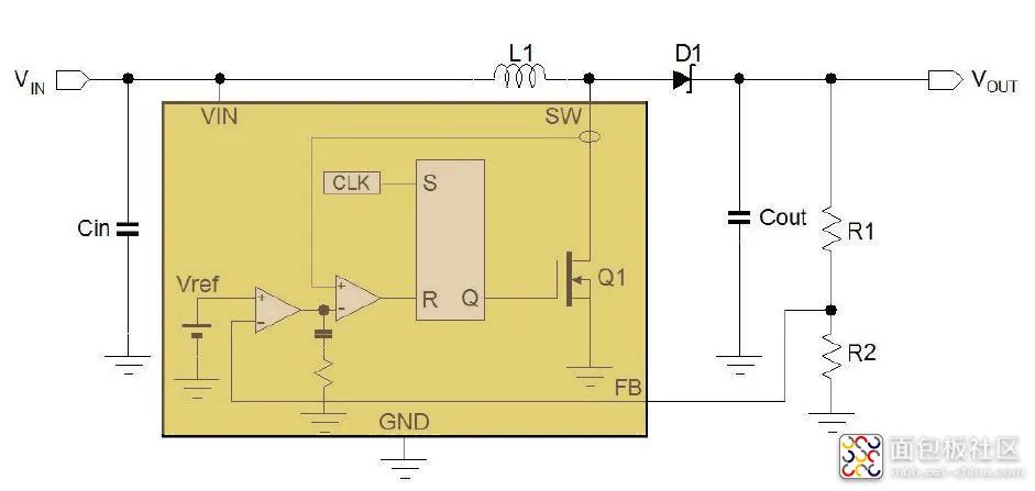
Basic Circuit Diagram of Boost Converter
The ON/OFF duty cycle of the MOSFET switch will determine the boost ratio VOUT/VIN, and the feedback loop also controls the duty cycle to maintain a stable output voltage. The output capacitor serves as a buffer element to reduce the output voltage ripple. The absolute maximum rating of the MOSFET current and the boost ratio together determine the maximum load current, while the absolute maximum rating of the MOSFET voltage determines the maximum output voltage. Some Boost converters integrate the rectifier with a MOSFET internally to achieve synchronous rectification.

Boost Converter with Four Internal Switches
Boost-Buck converters are used when the input voltage may change and can be lower or higher than the output voltage. When VIN is higher than VOUT, four internal MOSFET switches will automatically configure as a Buck converter, and when VIN is lower than VOUT, it will switch to Boost operation mode. This makes Boost-Buck converters very suitable for applications powered by batteries, especially when the battery voltage is lower than the regulated output voltage, extending battery life. Because the four-switch Boost-Buck converter operates in a fully synchronous mode, it can achieve higher efficiency. The output current capability in Buck mode is higher than in Boost mode; because under the same load conditions, Boost mode requires higher switching current. The absolute maximum rating of the MOSFET voltage will determine the maximum input and output voltage range. In applications where the output voltage does not need to reference ground, such as LED drivers, a Boost-Buck converter with only a single switch and a rectifier can be used. In most cases, the output voltage references VIN.
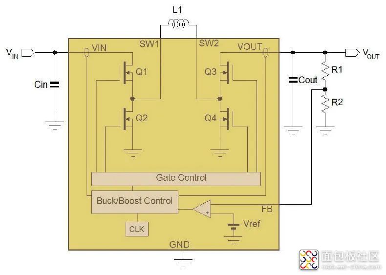
Boost-Buck Converter with Four Internal Switches
Most power management components use one of the four converter architectures mentioned above. For some special applications requiring very high switching currents (such as >10A), consider using external MOSFET modes. If monitoring power supply over-voltage or under-voltage conditions is required, specialized power monitoring ICs can be used.
References:
“AN027: Introduction to Power Management”, Richtek Technology, https://www.richtek.com
Author: Hard City Allchips, Source: Breadboard Community
Link: https://mbb.eet-china.com/blog/uid-me-3975615.html
Copyright Statement: This article is the original work of the blogger, and reproduction without permission is prohibited!

Electronic technology insights delivered promptly

-
Detailed article on RS-485 bus
-
Painful lessons from “Battery Voltage Detection Circuit,” including design key points
-
Faults caused by incompatibility of 3V and 5V levels
-
Domestic MCU, a showdown of champions
-
What circuit implements the button function of a television? Classic ADC button circuit
-
There are so many basic circuits in a small electric mosquito swatter, how many can you understand?