
The recent widespread trend is to utilize as many wireless communication technologies as possible on a single PCB. With the increase in wireless standards and the reduction in PCB size, it becomes challenging to understand what the most critical design parameters are.
This article will discuss the most important factors to consider when designing with hybrid wireless technologies such as Bluetooth, GPS, and Wi-Fi on a single PCB.
These considerations include antennas, frequency, FCC compliance, shielding, and layout with or without via transitions. Although the most common wireless standards have been mentioned, the following design considerations can apply to other wireless domains such as Z-Wave, LoRa, or Zigbee.

Author
Kirsten Zima
is an application engineer at Siemens EDA, providing support for layout and high-speed simulation tools.

Considerations for Antennas
One of the biggest design challenges for wireless products is the antenna. The reduction in size of wireless devices brings about the issue of reduced ground plane space required for the antenna. It is also possible to choose multiple antennas for each standard or to use dual-band or tri-band antennas for Wi-Fi and Bluetooth applications to save space.
In the case of using multiple antennas, the following factors should be considered: the increased likelihood of harmful cross-interference and the necessity of achieving the required polarity for directional design.
Additionally, is each antenna located inside or outside the final device enclosure? If it is internal, the composite materials of the enclosure will affect the signal. For example, polycarbonate has a strong attenuation.

The selected frequency (especially for Wi-Fi, as there are several available bands) will determine the length of the antenna—whether it is a full wave, half wave, or quarter wave—and matching the appropriate impedance is crucial for optimal performance.
Finally, the compactness of the design depends on the application of the final product. Is it for long-range or short-range applications? GPS is a long-range receiver that can capture signals from space satellites.
In contrast, Bluetooth is a short-range transceiver. The case design in Figure 1 illustrates a Bluetooth design. Other important antenna characteristics to consider include the gain, bandwidth, and radiation pattern required for each signal.
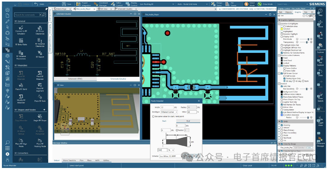
Figure 1: Design section of a Bluetooth wireless bent-F antenna in Xpedition
Chip antennas are very popular due to their small footprint and low loss. They are well-suited for mobile and higher frequency applications such as GPS and 2.4 GHz standards. When considering the use of chip antennas, it is crucial to follow the manufacturer’s design recommendations. A common misconception when using chip antennas is assuming that the chip components constitute the entire antenna, whereas, in fact, it requires an appropriate ground plane size to resonate correctly. Without a proper ground plane, the range of most antennas will be affected, especially for chip antennas.

RF Layout Recommendations
The antenna is just one of the factors to consider. Without proper impedance matching and RF design practices, one cannot expect the antenna to achieve optimal performance.
It is recommended to prioritize the design of RF layout first. Due to their outdoor radiation, they are the most critical nets. If the antenna routing is incorrect, both range and accuracy will be affected.
RF layout rules include having sufficient ground stitching vias along transmission lines, avoiding parallel placement of inductive components, and separating RF analog and digital ground nets by adopting a star structure. To achieve the best results, avoid excessively long RF routing paths.
RF traces should be short, straight, and the width should correspond to the required impedance from the RF source to the antenna. There are several reasons for this recommendation: to reduce losses, impedance variations, and harmful interference involving RF traces. Harmful interference is also a significant reason to keep high-speed networks away from RF traces.
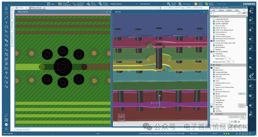
Figure 2: Complex via design created in Xpedition Layout to shield critical traces

Shielding Traces with Via Transitions
Sometimes longer RF traces are necessary, such as when a specific impedance is required. In such cases, proper shielding is key to protecting RF and high-speed nets from each other.
A common method for shielding RF lines is to use via transitions to bring RF between two ground planes, shielding potential EMI from the top and bottom. The via transitions should maintain impedance consistency with the traces, as any impedance mismatch will affect the signal and lead to signal degradation.
Other reasons for shielding include preventing EMI from interfering with other coexisting wireless and high-speed nets, as well as preventing unintentional radiation emissions that may impact FCC compliance requirements.
This is the most common reason for shielding, placing a metal box around the circuit, similar to a Faraday cage, to provide electromagnetic interference protection for the circuit.

Simulate Early and Often
It is important to understand whether the near field and far field are appropriate without spending time and money on multiple design iterations, and simulation of the design is strongly recommended.
Regardless of the simulation tool used, it is important to simulate several parameters of the circuit (far field and near field) to capture potential issues. The cost of redesigning the PCB multiple times is high. It is advisable to use simulation tools to achieve the expected design parameters for TX power output and RX sensitivity.
However, due to unforeseen factors, the final wireless design may differ from how it worked in simulation. This is why it is recommended to pre-screen and test the actual traces to see if they match the simulation.
Moreover, simulating the design before sample production can uncover significant issues, such as ensuring sufficient return loss, insertion loss, bandwidth, and expected gain.

FCC Compliance Details
Before bringing products to the U.S. market, all electronic devices that generate intentional or unintentional electromagnetic radiation must undergo compliance testing in an FCC-certified laboratory.
For the three main wireless standards, the following regulatory requirements in Part 15 must be adhered to.

1

GPS requires compliance testing for unintentional radiation under FCC Part 15.109, where there are field strength limits for each frequency range, and above 960MHz, the field strength must be below 500µV/m.

2

Bluetooth requires compliance testing for unintentional radiation under FCC Part 15.109 and for digital spread spectrum technology (DSSS) under FCC Part 15.247.

3

Wi-Fi requires compliance testing for unintentional radiation under FCC Part 15.109 and for DSSS under FCC Part 15.247.

4

Compliance with Part 15.247 prevents devices that emit intentional radiation from interfering with nearby wireless devices. It regulates devices that use spread spectrum and digital modulation in certain frequency bands, such as 2.4 GHz, which is most relevant to Bluetooth and Wi-Fi devices.

All three standards require checking the first ten harmonics during radiation to ensure they comply within restricted bands and within FCC radiation limits. Ensure that the device complies with FCC regulations before bringing it to market.

Benefits of Early Pre-Screening
Even if the product does not pass pre-screening, FCC compliance testing and certification require a one-time fee. Therefore, to ensure an effective path to market, it is recommended to pre-screen the design before certification and market release.
By pre-screening samples, issues can be identified early. This not only saves time during the product sample phase but also saves costs, not only due to the number of PCBs manufactured but also because the FCC laboratory may yield non-compliant results.
Pre-screening laboratories can also test according to the regulatory requirements of different countries to determine whether the design meets their requirements before sending it to those regions for licensing.
This does not mean it has been certified; it is merely testing its compliance before sending it to a certification laboratory. Since each region may have different EMI requirements for operating bands, the design must be tailored for the regions in which it will be used.
Some regions, such as Latin America, typically accept FCC documentation, while other countries, such as Australia, prefer to submit ETSI documentation for review. Finally, some countries, like Japan, will not accept FCC or ETSI test reports and require testing to be conducted domestically.
For the FCC, once a device is certified in an accredited laboratory, it will receive its unique FCC ID. Any minor changes to the device’s PCB or antenna will require retesting and re-certification.
A good practice is to consider any changes that may affect the potential radiation of the device, such as disabling an antenna or adding or changing a switching power supply. Examples of changes that do not constitute re-certification include replacing an LED.
Additionally, some standards have their own performance qualification certifications. Specifically for Bluetooth, devices must undergo qualification certification when registered with Bluetooth SIG. Using certified radio modules does not exempt one from FCC regulatory requirements for designs with multiple wireless technologies.

Conclusion
Regardless of the final application and design, the considerations and challenges discussed in this article are some of the major design factors that may be faced in wireless development.
In the final analysis, prioritizing and protecting RF circuits is a good practice. This is the most sensitive and tricky part of the design. RF design is referred to as “black magic” in the industry for a reason.








The above is a collaboration partner of the Chief Electronics Officer(partial)
Order does not imply priority