
The STDES-3KWTLCP reference design targets a 3 kW/53.5V AC-DC converter power supply for 5G communication applications, utilizing a complete ST digital power solution.
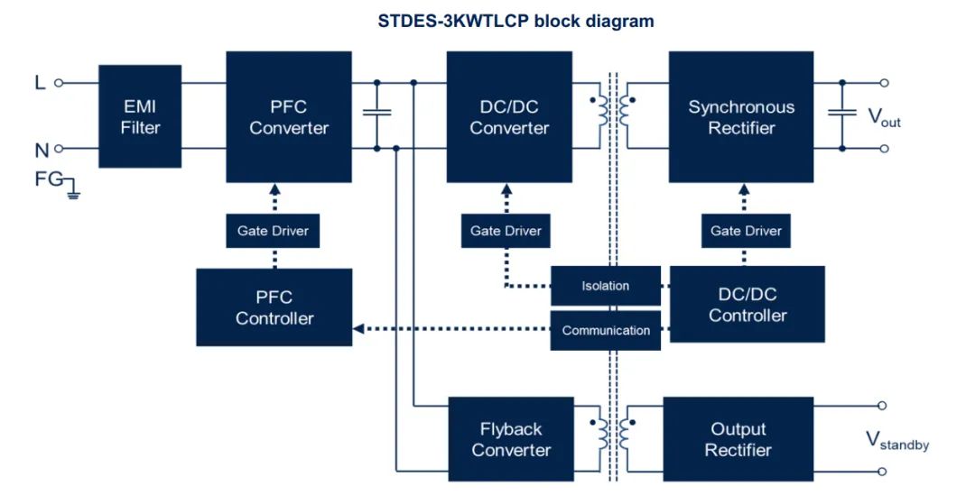
The circuit design includes a front-end totem pole PFC and a back-end LLC full-bridge architecture. The front totem pole PFC provides power factor correction (PFC) and harmonic distortion (THD) suppression, while the back-end full-bridge LLC converter provides safe isolation and stable output voltage.
This reference design is a high-efficiency, compact solution, achieving a peak efficiency of 96.3% at 230 VAC input, with low THD distortion (less than 5% THD at full load) and reduced material costs.
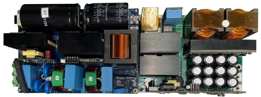
Its dimensions are 105 mm x 281 mm x 41 mm, with a power density of up to 40 W/in³.
The power supply consists of two power stages: one is a totem pole PFC controlled by the STM32G474RBT6 MCU, and the secondary is a full-bridge LLC + synchronous rectification (SR) also controlled by another STM32G474RBT6 MCU.
The STDES-3KWTLCP can also help users utilize ST’s latest power devices: third-generation semiconductor SiC MOSFETs, high-voltage MDmesh MOSFETs, super junction MOSFETs, isolated MOS drivers, and the VIPer series auxiliary power supplies.
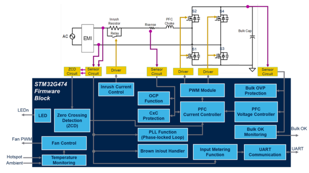
The principle of the front-end totem pole PFC controlled by the STM32G474RBT6 MCU is shown in the figure below:
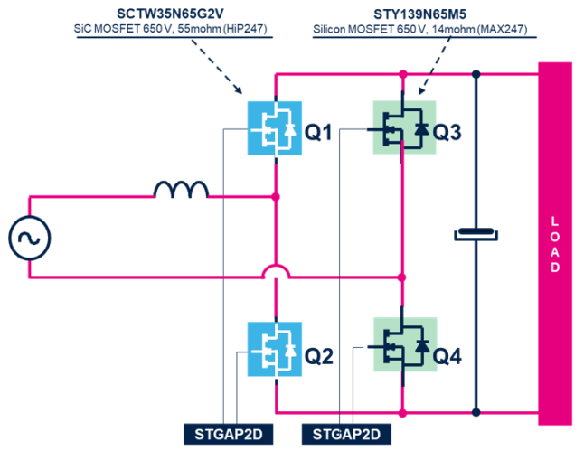
The architecture model of the totem pole PFC is shown in the figure below, where four MOSFETs are alternately turned on under the control of the MCU to achieve power factor correction. The two on the left must use third-generation wide-bandgap semiconductors such as SiC or GaN. In this case, the second-generation SiC SCTW35N65G2V from ST is used.
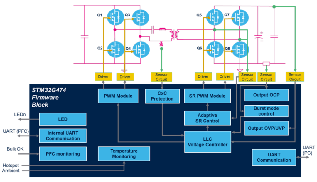
The principle of the LLC + SR controlled by the STM32G474RBT6 MCU is shown in the figure below:
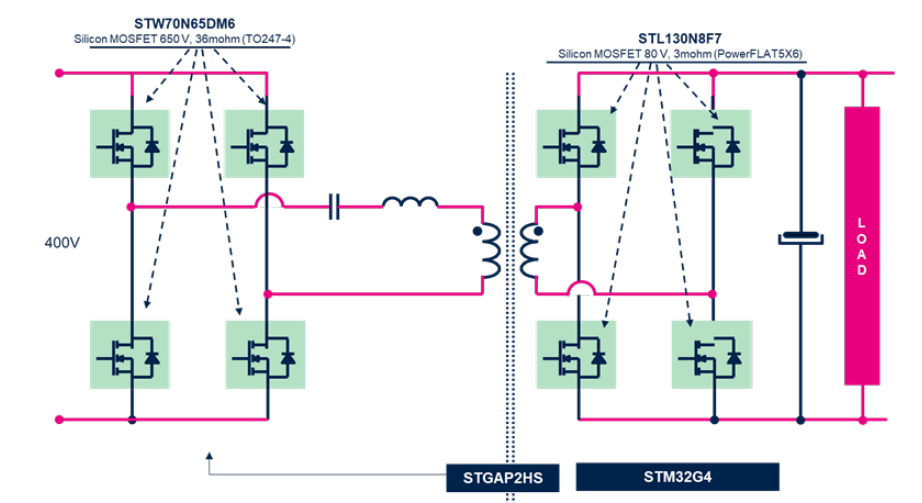
The architecture model of the full-bridge LLC is shown in the figure below, where four high-voltage MOSFETs on the primary side use ST’s low-loss M6 series super junction MOSFETs — STW70N65DM6, and four low-voltage MOSFETs on the secondary side use STL130N8F7 in a SMD 5*6mm package with a conduction resistance of 3mΩ.
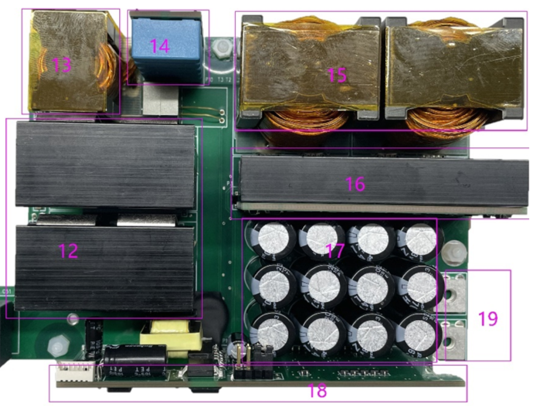
The distribution of the main power devices in the back-end LLC conversion section is shown below, featuring a very compact structure:
12–High-voltage MOS STW70N65DM6
13–Resonant inductor
14–Resonant capacitor
15–Main transformer
16–Secondary synchronous rectification low-voltage MOS
17–Output capacitor
18–MCU control small board
► Application Scenario Diagram

► Display Version Photo
► Solution Block Diagram
► Core Technical Advantages
• Utilizes ST SiC MOS (third-generation wide-bandgap semiconductor) for high temperature, low resistance, and low switching losses, with low body diode reverse recovery charge.
• Main control MCU chip ST32M474, fully digital design for power control.
• Power density reaches: 40 W/in³.
• High power factor & total harmonic distortion THD < 5% at full load.
• Peak surge current < 30A.
► Solution Specifications
• Input voltage: 90~264V
• Input voltage frequency: 47~63HZ
• Output voltage: 53.5V
• Output power: 3000W
• Power factor > 0.98 @ full load
• Peak efficiency 96.3%

Click to read the original text, download the technical document, and unlock over 1000 IoT, automotive, and power supply solutions, with over 700 technical experts from 大联大 online waiting for you. Click “See” to give the editor a thumbs up