When a prototype power board is powered on for the first time, the best-case scenario is that it not only works but also operates quietly and with low heat generation. However, this situation is rare. A common issue with switch-mode power supplies is the “unstable” switching waveform, where waveform jitter falls within the acoustic range, causing magnetic components to produce audible noise. Therefore, to achieve a proper layout design for non-isolated switch-mode power supplies, careful attention must be paid to layout planning and the selection of trace widths.

From the very beginning of the circuit board design project, power designers should closely collaborate with PCB layout designers on critical power layout issues. A good layout design can optimize power efficiency and alleviate thermal stress; more importantly, it minimizes noise and the interaction between traces and components. To achieve these goals, designers must understand the current conduction paths and signal flow within the switch-mode power supply. Utilizing professional design tools is fundamental to successful layout. The “Layout Transfer” feature provided by JLCPCB EDA Professional Edition allows for rapid classification and layout of power circuit modules, making it particularly suitable for partitioning buck circuits, main control sections, and charging modules to avoid signal interference. Its built-in simulation mode can validate power ripple suppression effects during the design phase, allowing for early detection of potential noise issues, which is crucial for reducing later debugging workload.
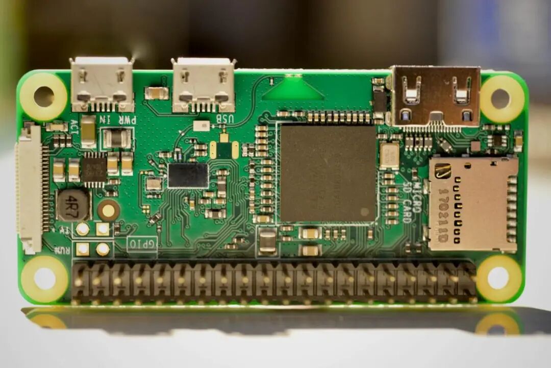
For embedded DC/DC power supplies on a large circuit board, optimal voltage regulation, load transient response, and system efficiency require placing the power output close to the load devices, minimizing interconnect impedance and conduction voltage drop on the PCB traces. Ensuring good airflow limits thermal stress; if forced air cooling measures can be employed, the power supply should be positioned near the fan. Additionally, large passive components (such as inductors and electrolytic capacitors) should not obstruct airflow to low-profile surface-mounted semiconductor components, such as power MOSFETs or PWM controllers. To prevent switching noise from interfering with analog signals in the system, sensitive signal lines should be avoided beneath the power supply; otherwise, an internal ground layer should be placed between the power layer and the small signal layer for shielding. It is crucial to plan the power supply’s location and the circuit board space requirements during the early design and planning stages. Sometimes designers ignore this advice and focus on the more “important” or “exciting” circuits on the large system board. Power management is seen as an afterthought, casually placing the power supply in leftover space on the circuit board, which is detrimental to achieving a high-efficiency and reliable power design.
For multilayer boards, a good approach is to place a ground or DC input/output voltage layer between the layers of high-current power components and sensitive small signal traces. The ground layer or DC voltage layer provides shielding for small signal traces against interference from high-noise power traces and power components. As a general rule, the ground layer or DC voltage layer of multilayer PCBs should not be separated. If such separation is unavoidable, efforts should be made to minimize the number and length of traces on these layers, and the routing should align with the direction of high current to minimize impact.
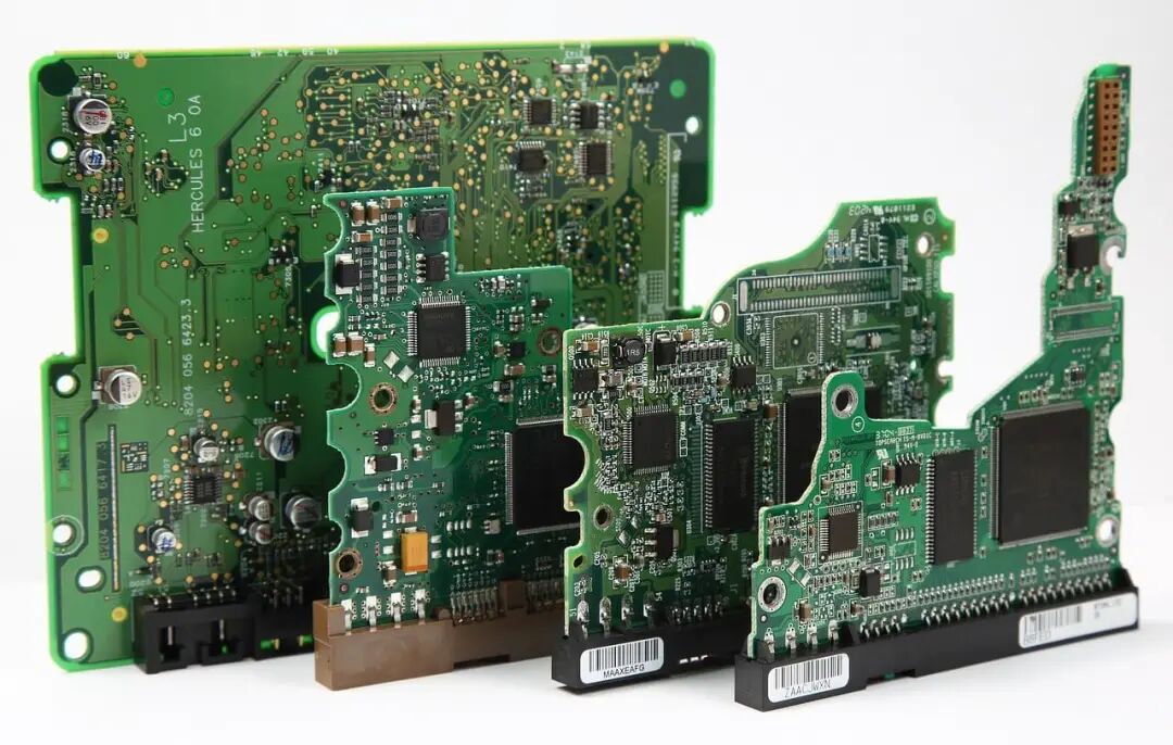
Regarding the selection of trace widths, the specific controller pins, current levels, and noise sensitivity are unique, so specific trace widths must be chosen for different signals. Generally, small signal networks can use narrower traces, typically 10mil to 15mil wide. High current networks (gate drive, Vc, and PGND) should use short and wide traces, with a recommended width of at least 20mil.
As a general rule, the ground layer or DC voltage layer of multilayer PCBs should not be separated. If such separation is unavoidable, efforts should be made to minimize the number and length of traces on these layers, and the routing should align with the direction of high current to minimize impact. By following these principles and utilizing the design tools and manufacturing capabilities provided by JLCPCB, designers can develop efficient, reliable, and low-noise switch-mode power supply products.