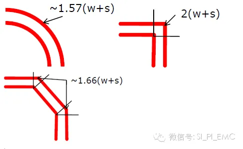
Question: In PCB routing, there are three common types of bends: right angle, 45 degrees, and arc (as shown in the figure below). Which type of bend is the best? This question can be answered relatively easily based on experience, with most people agreeing that arc > double 45 degrees > right angle. However, empirical observations cannot be definitive and are only valid within a certain range; only a full-wave electromagnetic field solver can accurately study this issue. Single-ended trace bends do not involve mode conversion, so we will take differential pairs as an example.
When a differential pair bends, the lengths of the inner and outer traces differ, leading to different signal delays. This is the main reason why some differential mode components convert into common mode components. However, the impedance discontinuity caused by the bend cannot be ignored either; a 2.5D electromagnetic field solver cannot calculate this effect.
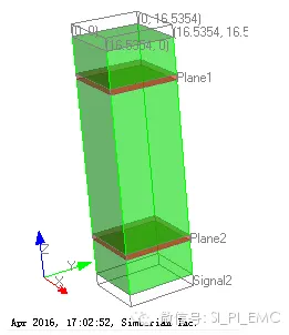
1. Layer Stackup
To study the above structure, a model was created in the 3D electromagnetic field solver Simbeor. A commonly used 4-layer board was selected, with material parameters: solder mask DK=3.3, LT=0.02, PP board Dk=3.3, LT=0.02, core DK=4.7, LT=0.02. The stackup is set as follows:
Cross-section of the board
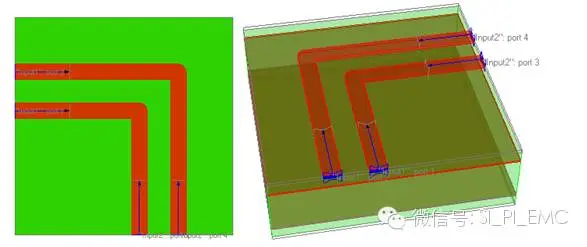
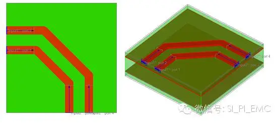
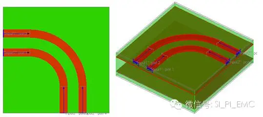
2. Structure
1. 90-degree corner:
Microstrip width 15 mil, spacing 22 mil, the length difference between the two traces is 209.5 mil.
2. 45-degree corner:
Microstrip width 15 mil, spacing 22 mil, the length difference between the two traces is 63 mil.
3. Arc corner:
Microstrip width 15 mil, spacing 22 mil, the length difference between the two traces is 59 mil.
 3. Simulation Results
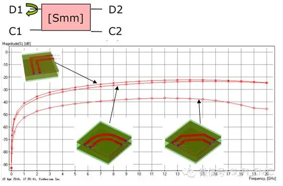
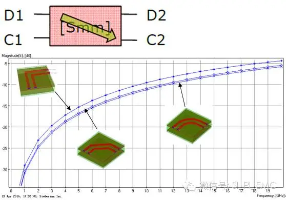
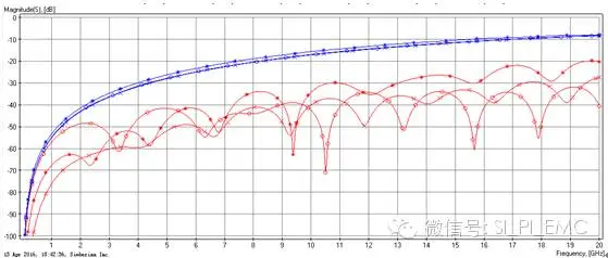
1. Differential mode reflection S[D1,D1]
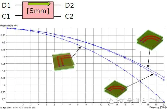
2. Differential mode insertion loss S[D1,D2]
3. Near-end mode conversion S[D1,C1]
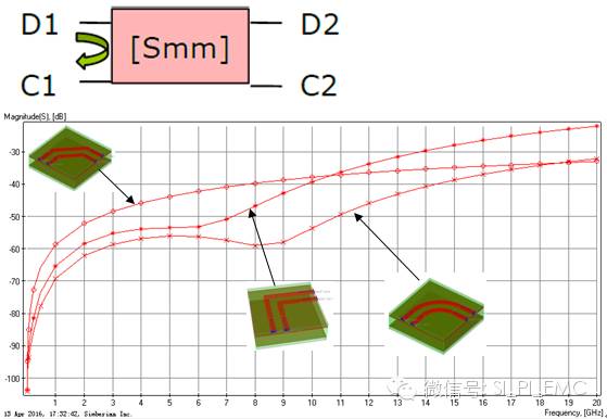
4. Far-end mode conversion S[D1,C2]
4. Conclusion:
1. The best differential mode return loss occurs at the 45-degree corner (not the arc), which may be unexpected for many;
2. The best differential mode insertion loss occurs at the arc corner, with 45 degrees being nearly as good, and 90 degrees being the worst. It is advisable to avoid 90 degrees in design;
3. For near-end mode conversion, the arc is the best. Surprisingly, in the frequency range below 10 GHz, the right angle performs better than 45 degrees;
4. For far-end mode conversion, the right angle is the worst, exceeding the other two by 1.4 dB. The arc and 45 degrees are very close. However, regardless of the type of bend, at 20 GHz, the far-end mode conversion reaches -5 dB, necessitating compensation for such bends in high-speed serial buses at 28Gbps/56Gbps.
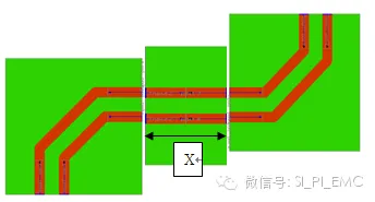
5. One way to compensate for the far-end mode conversion caused by bends is to use another bend in the opposite direction to create a center-symmetric trace layout. As shown in the figure below,x=250mil, the other two types of bends also require similar compensation:
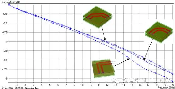
1. Differential mode insertion loss S[D1,D2]
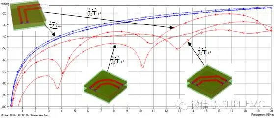
2. Mode conversion
In summary: 1. After compensation, the differential mode insertion loss at the 45-degree corner is slightly better than the arc across all frequency bands, with 90 degrees being the worst;
2. After compensation, the far-end mode conversion reaches -16 dB at 20 GHz, with the right angle being slightly worse than the other two. However, no matter how much compensation is applied, it cannot be reduced to a very low level. This is mainly because once mode conversion occurs, the propagation speed of common mode signals is slower than that of differential mode signals. Phase can be compensated, but propagation speed cannot be compensated with simple trace geometry. If the signal propagation speeds of the two modes are the same (internal strip line), the situation improves significantly.
What if x=1000 mil?
At this point, the far-end mode conversion suddenly reaches -8 dB, which is significant. This indicates that if differential pairs become mismatched due to routing, compensation must be applied quickly; the smaller the x value, the better the compensation effect. However, sometimes due to routing direction, there is only one bend. In this case, the following processing can be done, using a serpentine trace on the inner side to quickly restore the matching compensation.
[1]Interest-driven passion
[2] Should hardware engineers design their own PCBs?
[3]How long should PCB traces be?
[4]How wide should PCB traces be?
[5]Inner layers of PCBs
[6]Via holes
[7]Can PCBs have sharp angles and right angles?
[8] Should dead copper be retained? (PCB islands)
[9]Can vias be placed on pads?
[10] PCB materials, what does FR4 actually refer to?
[11] Solder mask, why is green oil mostly green?
[12]Steel mesh
[13]Pre-layout
[14]Key points of PCB layout and routing
[15] Cross-segment routing
[16] Signal reflection
[17] Dirty signals
[18] Surface treatment processes such as gold plating, immersion gold, and tin spraying
[19] Trace spacing
[20] Placement of capacitors
[21] Crosstalk
[22] Flying probe testing of PCBs
[23] Overview and simulation of FPC
[24] Why do PCBs deform and bend? How to solve it?
[25] Understanding “characteristic impedance” in one article
[26] PCB stackup design
[27] High-speed circuit PCB return paths
[28] Power handling and plane segmentation in PCB design
[29] Zigzag PCB routing – Tabbed routing
[30] What is the dielectric loss angle in PCBs?
[31] The impact of PCB copper foil roughness on high-speed signals
[32] Why should crystal oscillators not be placed at the edge of PCBs?
[33] What are high-speed signals?
[34] What is a transmission line?
[35] Pre-emphasis, de-emphasis, and equalization
[36] How to utilize PCB heat dissipation
[37] “Stub” in PCB design
[38] Dilemma: Should there be a GND protection line between traces?
[39] PCB copper pour
[40] Rules to follow when designing PCBs
[41] “Fake eight-layer” in PCB stackup design
[42] Besides strip lines and microstrip lines, there are also “coplanar waveguides”
[43] Relevant parameters of PCB pad design processes
[44] Why should grounding holes be drilled at the edges of PCBs?
[45] PCBs that are easier to dissipate heat: aluminum substrates
[46] Why should reference planes be hollowed out?
[47] PCB design for crystal oscillators
[48] Designing DC/DC power supply PCBs with EMC considerations