The sampling rate refers to the speed at which an Analog-to-Digital Converter (ADC) samples the analog input, or the speed at which a Digital-to-Analog Converter (DAC) outputs the analog signal. This rate is typically provided by the external clock rate to these converters. However, modern ADCs and DACs often have an internal Phase-Locked Loop (PLL) that offers the option to use a slower input clock to generate a high-speed sampling clock.The data rate refers to the rate of digital output data from the Analog-to-Digital Converter (ADC) or the digital input data rate for the Digital-to-Analog Converter (DAC). In many cases, these rates are not the same as the sampling clock rate.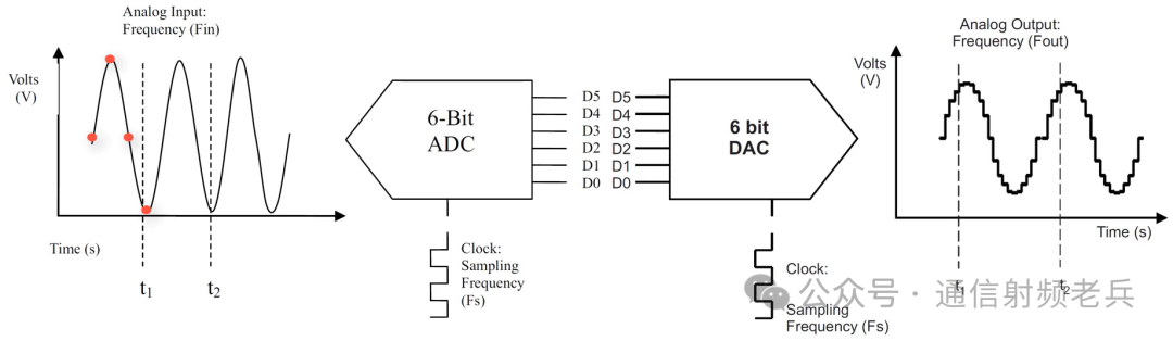
For example, a 16-bit ADC operating at a sampling rate of 1 Gsps in a decimation factor of 2 mode will have an actual data rate output of1 Gsps sampling rate divided by 2, which equals 500 Msps. If the user operates in a decimation factor of 4 mode, the data rate will be250 Msps.
It is important to note that this is the equivalent parallel data rate, not the serial output rate of the device’s output pins, which is related to the serializer/deserializer (SerDes) rate. This will be discussed later. For new high sampling rate data converters, higher data rates are required. In many cases, these rates are too high for data converter devices or for Field Programmable Gate Arrays (FPGAs) or Application-Specific Integrated Circuits (ASICs) that receive data from or provide data to the data converters.
Another reason may be the number of available input/output (I/O) channels. In either case, the data rate often needs to be reduced. To achieve this, interpolation and decimation techniques are employed. When using decimation or interpolation, a good rule of thumb is to choose a data rate that can support the signal bandwidth and a sampling rate that can support spectral purity.
Next, we will discuss the relevant concepts of decimation. This will include its definition, comparison of time and frequency, advantages and disadvantages, and examples of specific devices.
What exactly is decimation? In digital signal processing, decimation is the process of reducing the sampling rate of a signal. The term “downsampling” typically refers to a step in this process, but sometimes the two terms can be used interchangeably. Complementary to upsampling or interpolation, decimation is a specific case of sampling rate conversion in multi-rate digital signal processing systems.
When performing decimation on a sequence of sampled signals or other continuous functions, it produces an approximation of a sequence, as if the signal were sampled at a lower sampling rate. This is achieved by removing sample points from the data stream. Decimation typically passes through a digital low-pass filter or anti-aliasing filter before the decimation operation.
This operation is similar to using an analog anti-aliasing filter with a center frequency equal to the sampling rate divided by the decimation factor. The decimation factor is usually an integer greater than 1 or a rational fraction. This factor is used to divide the sampling rate or is equivalent to multiplying the output data rate by this number to determine the actual sampling rate used by the Analog-to-Digital Converter (ADC).
Decimation is used to reduce the sampling rate to a level that the device can handle, allowing for higher sampling rates to achieve more flexible frequency planning and improving spectral performance through filtering.
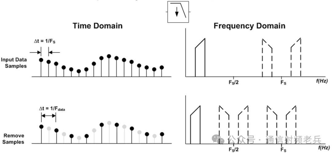
The following figure illustrates examples of the decimation function in both the time and frequency domains. When performing decimation, mirror signals are produced, as shown in the frequency domain graph. In this example, the signal and mirror signals around the sampling rate are shifted down to half the sampling rate. Signals and mirror signals at a sampling rate of 2 times Fs will shift down to Fs, and so on. A low-pass filter is then used to provide anti-aliasing protection, which will remove these mirror signals and yield a clean spectrum at a much lower data rate.
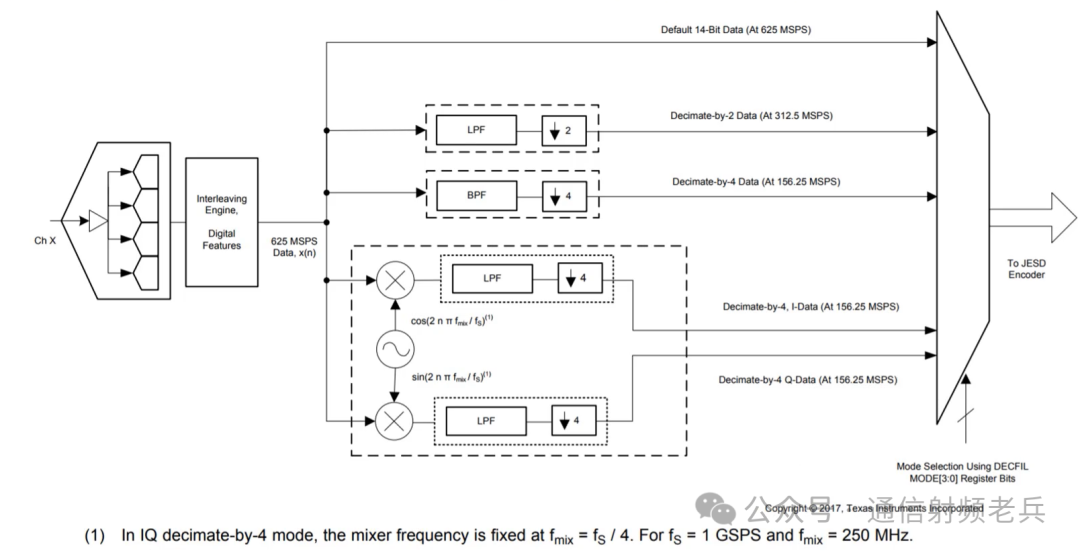
Data sheets typically include block diagrams showing the available functions of the Digital Down Converter (DDC). The following diagram illustrates an example of the digital down converter functionality available internally in an Analog-to-Digital Converter (ADC). From this diagram, it can be seen that this device offers several functions, including modes with a decimation factor of 2, a decimation factor of 4, followed by mixer shift options for the decimation factor of 4 module, and a bypass mode for the digital down converter.
As mentioned earlier, decimation is accompanied by filtering, which can be seen from this block diagram. This device provides options for low-pass or high-pass filters in the decimation factor of 2 mode. In the decimation factor of 4 mode, it offers four different center frequency options for band-pass filtering.
Using decimation has both advantages and disadvantages. Advantages include providing signal-to-noise ratio (SNR) processing gain, maintaining the frequency domain view of the signal, reducing noise power through the decimation filter, improving SNR performance, and reducing overall noise in the converter due to averaging the samples. However, using decimation is not without its costs. Some disadvantages include the need for more digital logic. Using more digital logic consumes more power and reduces overall signal bandwidth capability.
What is interpolation? In digital signal processing, interpolation (or upsampling) is the process of increasing the signal sampling rate without affecting the signal itself. Interpolation is a method of constructing new data points within the range of a set of discrete known data points.
A typical method for performing interpolation is as follows: insert a logical 0 between each sample point. This is called zero insertion or upsampling. Filter the mirror signals produced by the upsampling process. This will achieve 2x interpolation. To achieve 4x interpolation, repeat this process again. To achieve 8x interpolation, repeat once more, and so on. This cascading method is preferable as it improves the efficiency of the required half-band filters.
Through interpolation, the output rate of the Digital-to-Analog Converter (DAC) can be increased. The mirror signals can be moved further away from the target frequency band of interest, allowing for a wider Nyquist region and enabling the DAC to maintain a reasonable digital data rate.
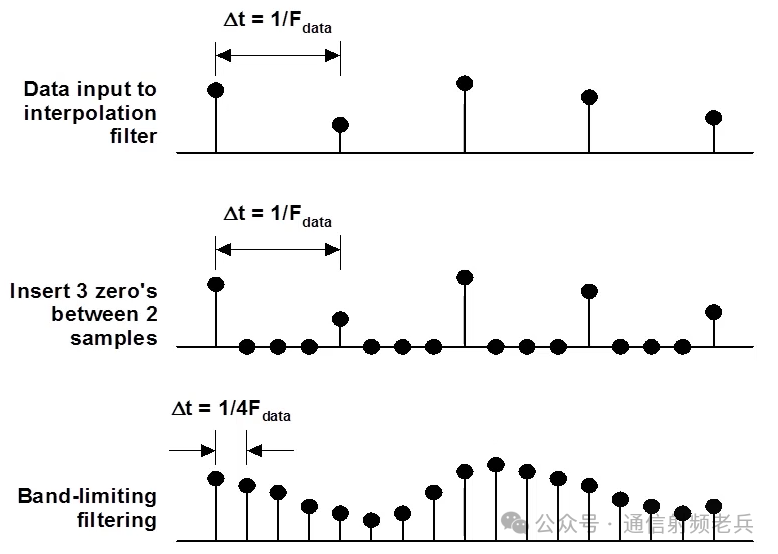
The following figure illustrates the function of interpolation in the time domain. This example shows that three zeros are inserted between the original sample points. Adding zeros does not change the spectral content of the signal; it merely widens the bandwidth. Then, filtering methods such as low-pass filters are used to adjust the added sample points to fill in the missing levels between the actual sample points, as shown in the bottom graph.
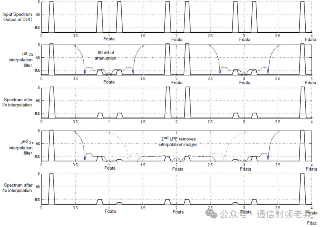
The following figure shows the view of interpolation in the frequency domain. The top graph is the typical output of a digital upconverter after adding zeros to the original data, but before applying any filtering. The second graph shows the effect of a 2x interpolation low-pass filter. This filter will be used to attenuate the mirror signal data around Fdata. Typically, if greater than 2x decimation is required, it will be done in stages.
The third graph illustrates the effect of a second 2x interpolation stage used in the signal chain to achieve 4x interpolation. The fourth graph shows the result after processing with the second low-pass filter of the second stage. Using these two low-pass filters allows the output signal’s tone to remain unchanged while achieving a much higher sampling rate, as shown in the bottom graph. Now, if needed, the user can use a Numerically Controlled Oscillator (NCO) to shift this original signal to a much higher intermediate frequency (IF) with minimal performance degradation.
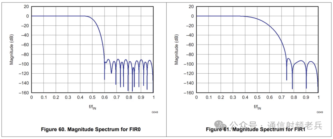
The device’s data sheet should display the finite impulse response (FIR) filter response of the device’s interpolation filter. The following figures 60 and 61 show the magnitude frequency response of the FIR0 and FIR1 interpolation filters used by a certain DAC.
The horizontal axis uses a normalized scale relative to the FIR filter input data rate. Other charts that can be found in the device data sheet include the composite filter response of the entire cascaded interpolation module used. Note that when the frequency of interest approaches the filter’s cutoff frequency, there will be a loss in signal amplitude, which will lead to a reduction in signal-to-noise ratio (SNR). Additionally, using multiple FIR filters will add latency to the data path. These latency values are typically listed in the data sheet.
Using interpolation has both advantages and disadvantages. The advantages include moving the mirror signals of the Digital-to-Analog Converter (DAC) further away from the frequency band of interest, making output filtering easier. It allows for a wider Nyquist region for flexible frequency planning, reduces noise spectral density, lowers the required input data rate, and achieves higher output sampling rates.
However, using interpolation is not without its costs. Some disadvantages include the need for more digital logic, which consumes more power and increases latency, and the input bandwidth being limited by the interpolation filter, such as BW=0.4*Fdata.
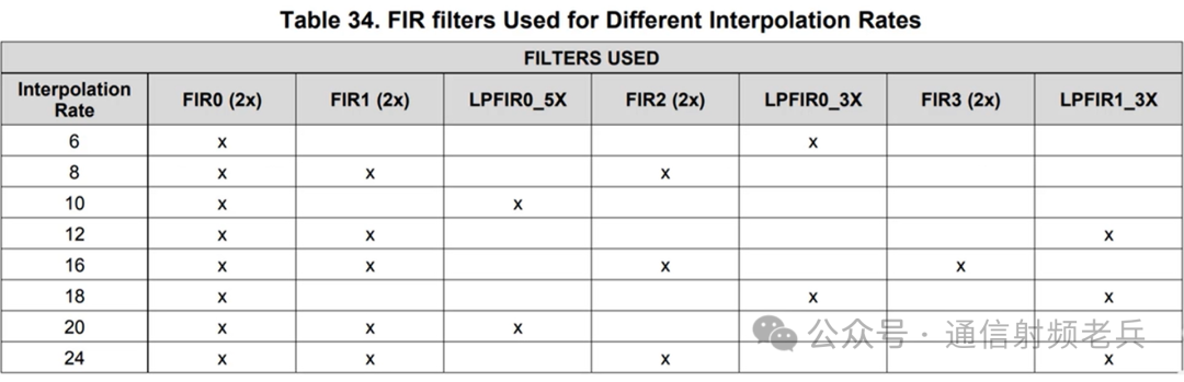
The following figure is an example of a Digital-to-Analog Converter (DAC) device with internal interpolation functionality. As shown, this feature allows for several different interpolation rates. This table also shows users the filters used to achieve each interpolation rate.
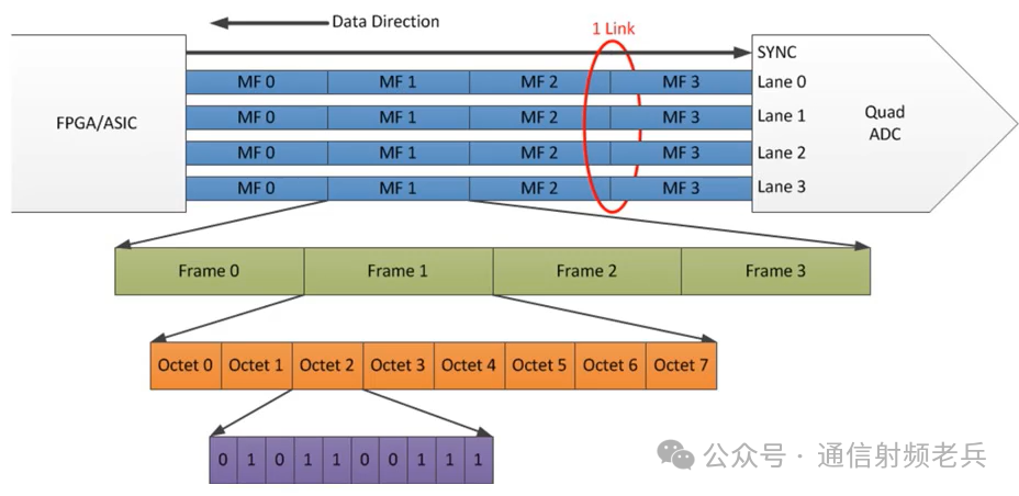
Next, we will discuss the sampling of new high-speed data converters using the JESD204B standard. JESD204B is a standardized serial interface between data converters and logic devices such as Field Programmable Gate Arrays (FPGAs) or Application-Specific Integrated Circuits (ASICs), and is adopted by most new high-speed data converters being developed today.
With this new standard, JESD204B devices can easily sample in the GHz range. Some newer RF Digital-to-Analog Converters (RFDACs) can have sampling rates of up to 9 Gsps. Sampling at such rates has its drawbacks, as it requires each serializer/deserializer (SerDes) channel to have an input data rate of 90 Gbits per second. Since the JESD204B standard only supports a maximum rate of 12.5 Gbits per second, the data rate must be reduced. To achieve this, interpolation techniques need to be employed.
Many JESD-compliant Digital-to-Analog Converters (DACs) offer multiple options for selecting the interpolation factor. This gives users more choices when selecting the number of serializer/deserializer (SerDes) channels needed and the operating speed of those channels. For current JESD204B Analog-to-Digital Converters (ADCs), this is not a significant issue as their sampling speeds are not as high. However, if users want to reduce the number of channels, this can become a problem and decimation operations will be required.
In this example, we demonstrate a DAC that will use all 4 DACs, 8 serializer/deserializer channels, with an interpolation factor of 4, and a maximum sampling rate of 2.5 Gsps. To determine if the serializer/deserializer rate is within the specifications of the JESD204B standard, we will perform the following calculations.
First, we convert the 8-bit bytes used in JESD204B to bits. Since each sample value consists of two bytes, the sampling rate Fs=2.5 Gsps/4=625 Msps, and each DAC will have 1250 M bytes per sample value. JESD204B uses 8b/10b encoding, so each byte will consist of 10 bits. Thus, we arrive at a total of 12500 Mbps.
Now the total bit rate is 12500 Mbits per second multiplied by 4 DACs, which equals 50 Gbps. To keep this rate below 12.5 Gbps, we choose 8 serializer/deserializer channels, reducing it to 6.25 Gbps. Another option is to use 4 channels, which would bring the rate to 12.5 Gbps. This is where the customer needs to weigh their options—using more channels but at a slower speed, or using fewer channels but at a much higher rate. They cannot use fewer than 4 channels, as this would exceed the data rate specifications for the serializer/deserializer in the JESD204B standard.
So ultimately, the JESD204B configuration is set to LMFS=8411, Lane rate=6.25 Gsps.
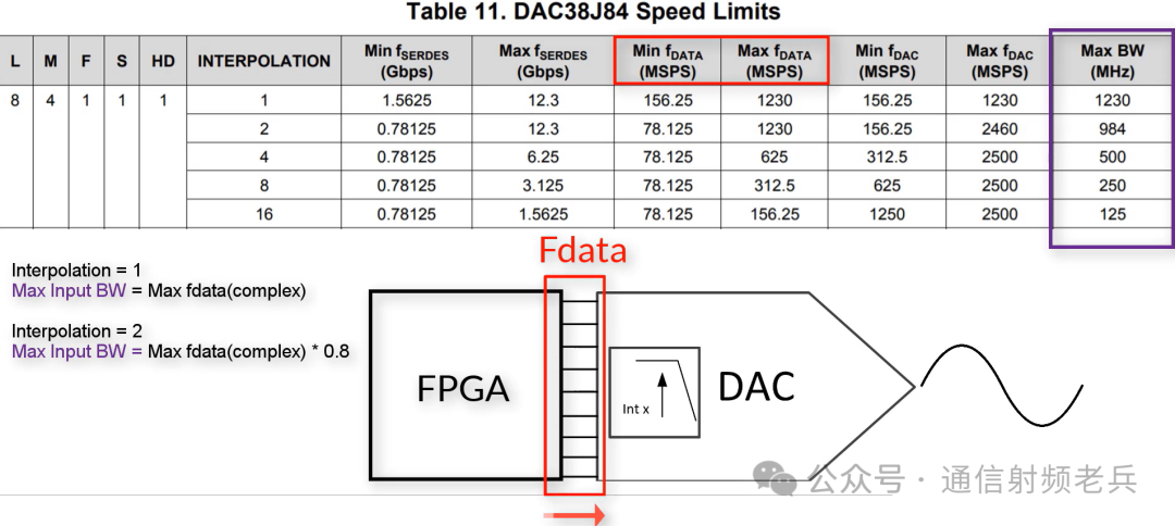
In the following figure, you will see a table showing the minimum and maximum sampling rates that this Digital-to-Analog Converter can use. fData is the rate at which parallel data leaves the JESD204B module and enters the digital input module of the DAC. fDAC is the actual sampling rate of the DAC. fDAC equals fData multiplied by the interpolation factor. Since the serializer/deserializer outputs use an internal Phase-Locked Loop (PLL), they will have a minimum and maximum operating range. Therefore, JESD204B data converters have a relatively high minimum sampling rate. In many cases, to use the maximum sampling rate, users must employ some interpolation operations to reduce the serializer/deserializer rate to below 12.5 Gbps, which is the maximum rate allowed by the JESD204B standard.