Introduction:Everyone knows that impedance should be continuous. However, as Luo Yonghao said, “In life, there are always times when you step in something unpleasant,” PCB design also has its moments of impedance discontinuity. What should we do?
Characteristic Impedance
Characteristic Impedance: Also known as “Feature Impedance”, it is not a DC resistance, but a concept in long-line transmission. In the high-frequency range, during the signal transmission process, as the signal reaches its destination, an instantaneous current is generated between the signal line and the reference plane (power or ground plane) due to the establishment of an electric field.
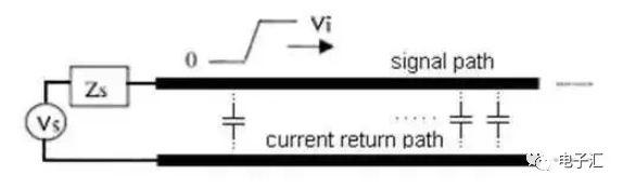
If the transmission line is isotropic, then as long as the signal is being transmitted, there will always be a current I. If the output voltage of the signal is V, during the signal transmission process, the transmission line can be equivalently treated as a resistor, with a magnitude of V/I. This equivalent resistance is referred to as the characteristic impedance Z of the transmission line.
During the transmission of the signal, if the characteristic impedance along the transmission path changes, reflections will occur at the nodes of impedance discontinuity.
Factors Affecting Characteristic Impedance
The factors affecting characteristic impedance include: dielectric constant, dielectric thickness, line width, copper foil thickness.
2.1 Gradient Line
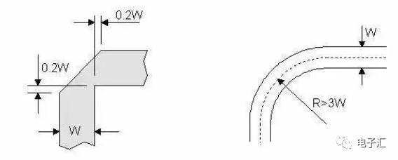
Some RF device packages are small, and the SMD pad width may be as small as 12 mils, while the RF signal line width may exceed 50 mils. Gradient lines should be used to prevent abrupt changes in line width. The gradient line is shown in the figure, and the transition part should not be too long.
2.2 Corners
If the RF signal line makes a right angle, the effective line width at the corner will increase, causing impedance discontinuity and signal reflection. To reduce discontinuity, corners should be treated using two methods: chamfering and rounding. The radius of the arc should be sufficiently large; generally, it should ensure: R>3W. As shown in the figure below.
2.3 Large Pads
When there are large pads on a 50-ohm microstrip line, the large pad acts as a distributed capacitor, disrupting the continuity of the microstrip line’s characteristic impedance. Two methods can be employed to improve this: first, increase the thickness of the microstrip line dielectric, and second, excavate the ground plane beneath the pad, both of which can reduce the distributed capacitance of the pad. As shown in the figure below.
2.4 Via
A via is a metal cylinder that is plated between the top and bottom layers of the circuit board. Signal vias connect transmission lines on different layers. Via stubs are the unused portions of the via. Via pads are annular pads that connect the via to the top or internal transmission lines. Isolation pads are annular gaps within each power or ground layer to prevent short circuits to the power and ground layers.
● Parasitic Parameters of Vias
Through rigorous physical theoretical derivation and approximate analysis, the equivalent circuit model of a via can be represented as an inductor with a grounding capacitor in series at both ends, as shown in the figure below.
● Equivalent Circuit Model of Vias
From the equivalent circuit model, it can be seen that the via itself has parasitic capacitance to ground. Assuming the diameter of the via pad is D2, the diameter of the via pad is D1, the thickness of the PCB is T, and the dielectric constant of the substrate is ε, the parasitic capacitance of the via can be approximated as:
The parasitic capacitance of the via can lead to extended signal rise times and reduced transmission speeds, thereby degrading signal quality. Similarly, vias also have parasitic inductance, and in high-speed digital PCBs, the hazards posed by parasitic inductance often outweigh those of parasitic capacitance.
Its parasitic series inductance can weaken the contribution of bypass capacitors, thereby diminishing the filtering effectiveness of the entire power system. Assuming L is the inductance of the via, h is the length of the via, and d is the diameter of the center drill hole, the approximate size of the parasitic inductance of the via is:
Vias are one of the significant factors causing impedance discontinuity on RF channels. If the signal frequency exceeds 1GHz, the impact of vias must be considered.
Common methods to reduce via impedance discontinuity include: using via-less technology, selecting appropriate routing methods, and optimizing the pad diameter. Optimizing the pad diameter is a commonly used method to reduce impedance discontinuity. Since the characteristics of vias are related to the dimensions of the hole diameter, pad, anti-pad, stacking structure, routing methods, etc., it is recommended to perform optimization simulations using HFSS and Optimetrics based on specific conditions for each design.
When using a parametric model, the modeling process is straightforward. During the review, PCB designers need to provide the corresponding simulation documentation.
The diameter of the via, pad diameter, depth, and anti-pad will all bring changes, causing impedance discontinuity, reflection, and the severity of insertion loss.
2.5 Through-Hole Coaxial Connectors
Similar to the via structure, through-hole coaxial connectors also exhibit impedance discontinuity, so the solutions are the same as for vias. Common methods to reduce impedance discontinuity in through-hole coaxial connectors include: using via-less technology, appropriate routing methods, and optimizing the pad diameter.
 |
Share technical articles, news, and communication meetings related to electronics Subtle progress every day Gathering electronic technology |