Modern embedded devices are highly advanced, with embedded systems interacting with external human-machine interfaces. Currently, touch screens are popular, and even in the wave of AI, compact embedded devices can directly accept voice input for AI recognition, allowing a simple phrase like “Old Wu, please help me with xxx” to suffice. 
However, in scenarios requiring highly reliable interaction, such as industrial automation or medical devices, traditional mechanical contact devices represented by mechanical switches and relays still hold an irreplaceable position in various devices due to their unique advantages.
 When using the signal from a mechanical switch as input, the inherent physical characteristic—”bounce”—must be taken seriously and properly handled. Bounce refers to a series of high-speed, unstable on-off phenomena that occur due to the elastic collision of metals at the moment the mechanical contacts close or open. For the digital input pins of a microcontroller, each on-off transition may be misinterpreted as a valid signal edge. For example, a single button press should only trigger one interrupt or count once, but due to bouncing, it may be incorrectly recognized as dozens of times within a few milliseconds, leading to logical confusion or system instability.
The above figure shows a typical bounce waveform generated at the moment the mechanical contacts close. It can be seen that before the signal stably switches from high level (OFF) to low level (ON), it experiences a period of instability lasting several milliseconds, during which the signal level oscillates violently between low and high levels. The duration and amplitude of this oscillation vary depending on factors such as the type of switch, its age, and the driving force, but its existence is fatal for high-speed responsive digital circuits.
To address the bounce issue, the industry has developed various mature solutions, mainly divided into hardware and software categories.
Software Debouncing
This is likely the first method we encounter when learning embedded development, as the development boards we purchase for learning do not add hardware debouncing circuits, making software debouncing the lowest-cost method. The core idea is to implement “secondary sampling delay filtering” through software. When the input pin level changes for the first time, the program does not respond immediately but instead starts a brief delay (usually 10-20ms, longer than the maximum bounce time). After the delay, the level of the pin is read again. If the level at this time is consistent with the level after the first change, it is confirmed as a valid state change. This method is simple and effective but consumes CPU resources, and during the delay, the program cannot respond to other tasks (unless using interrupts or timers), making it unsuitable for some real-time applications.
Hardware Debouncing
Using digital logic devices, such as an RS flip-flop (Set-Reset Latch) made from NAND gates, can achieve pure hardware debouncing. Utilizing the bistable characteristic of the flip-flop, the first contact of the switch can lock the output state, and subsequent bounces will not affect the output result until the contact touches the other end, causing a state flip. This method is fast in response and does not consume software resources, but it is only effective for single-pole double-throw (SPDT) switches with normally open (NO) and normally closed (NC) contacts, and it cannot suppress noise interference from outside the circuit.
When designing debouncing circuits or writing debouncing algorithms, the most common question we ask is: “How long will the bounce last?” Many designs circulating on the internet often rely on some empirical rules or “ancestral code” without solid experimental data support. However, the characteristics of bounce are far more complex than a simple “maximum bounce time.” What does the waveform on the input pin look like during the bounce? What are its specific characteristics? Without understanding the complete characteristics of the input signal, rashly writing processing functions is extremely dangerous for building high-reliability systems.
Therefore, any reliable debouncing solution should be based on a deep understanding of the switch bounce behavior, and this understanding must come from actual physical measurements and data analysis.
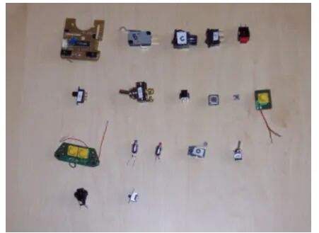
To obtain precise bounce data, the expert Jack Ganssle conducted a series of experiments on this website [1]. The subjects of the experiments included 18 different types of switches, including commonly used momentary buttons, toggle switches, slide switches, and even micro switches taken from old game controllers and mice. The experimental data is comprehensive and representative, allowing us to fully understand the physical phenomenon of bounce. Here, Old Wu cites the experimental results of Jack Ganssle.
The core of the experimental setup described on the website is a microcontroller development board and a mixed-signal oscilloscope (MSO). The initial plan was to use the microcontroller to directly capture the level changes of the switch pin, but Jack Ganssle quickly discovered the limitations of this method. Many switches exhibit bounces that include ultra-narrow pulses with durations less than 100 nanoseconds, and the conventional microcontroller sampling rate struggles to accurately capture these transient details.
Therefore, the final observation was conducted using a mixed-signal oscilloscope (MSO). The MSO can simultaneously capture analog waveforms and digital logic levels, allowing us to see not only the continuous changes in voltage but also understand how digital circuits interpret this noisy analog signal. The test circuit is very simple: a 5V power supply is connected to the switch through a 1kΩ pull-up resistor, and the oscilloscope probe directly measures the voltage at the switch pin.
The experimental results revealed several key characteristics of switch bounce:
1. Significant Variability in Bounce Duration: Most switches have bounce durations within a few milliseconds. Among all 18 samples, excluding two extreme outliers, the average bounce duration for 16 switches was 1.557ms, with a maximum of 6.2ms. However, there are exceptions, such as a seemingly ordinary red button switch (Sample E), which recorded a bounce duration of up to 157ms when the contacts opened.
2. Inconsistent Behavior Between Closing and Opening: Seven switch samples exhibited bounce durations when closing that were significantly longer than when opening. For most switches, the bounce during opening is usually very brief, even less than 1 microsecond, but in the next operation of the same test, the bounce duration may leap to several hundred microseconds, showing a high degree of randomness.
3. Individual Variability Among Same Model Switches: The experiment tested two pairs of switches of the same model, and the results showed that their bounce characteristics could differ by as much as twofold. This warns us that in product design, we cannot rely solely on the test data of a single device; we must consider the individual variability of components.
4. Operation Method Affects Bounce: The way a switch is pressed (e.g., fast or slow, light or heavy) also affects bounce behavior. For example, quickly toggling a toggle switch (Sample G) produces a bounce duration three times that of toggling it slowly. This simulates real-world usage scenarios, such as a user frantically pressing a button or the device experiencing vibrations.
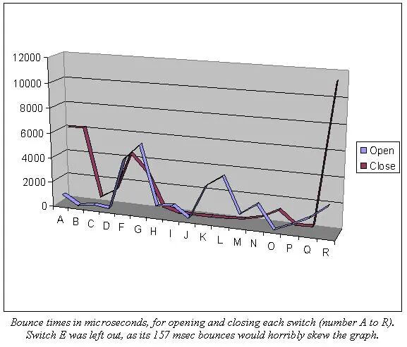
Figure. Distribution of Bounce Durations for Different Switch Samples
Through the MSO’s analog channel, we observed more waveform details than pure digital logic. A few switches can produce nearly ideal transitions between 0V and 5V, but most switches exhibit much more complex electrical behavior.
A typical phenomenon is “contact wiping.” At the moment the contacts separate, they do not immediately disconnect but instead undergo a brief sliding or rolling process on each other’s surfaces. During this process, the contact resistance does not abruptly change from zero to infinity but increases smoothly, exhibiting variable resistance. For example, when switch C opens, its equivalent resistance rises linearly from 0Ω to 6Ω over 150µs before suddenly transitioning to an open state. This results in its output voltage showing a slow ramp rather than a steep step.
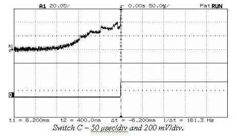
Figure. Voltage Slowly Ramping Up When Switch C Opens, Exhibiting Contact Wiping Behavior
This slowly changing analog signal poses a severe challenge to digital inputs. For example, according to TTL level standards, 0V to 0.8V is recognized as logic “0”, while above 2.0V is recognized as logic “1”, and the range between 0.8V and 2.0V is the “uncertain region.” When the switch voltage hovers in this uncertain region, the logic gate circuit at the digital input may oscillate, outputting a series of uncertain, rapidly changing 0s and 1s, as if the switch were bouncing at high speed.
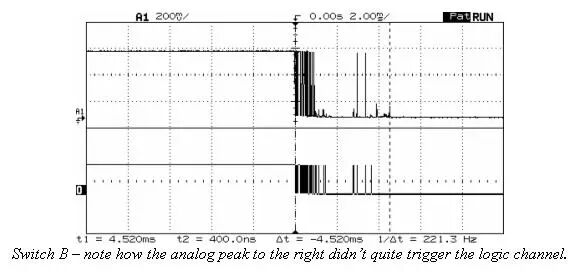
Figure. The Voltage of Switch B Hovers in the TTL Uncertain Region, Causing Digital Logic Output to Oscillate
Interestingly, some conductive rubber switches (commonly used in remote controls and other consumer electronics) produce a very smooth voltage ramp from 0V to 5V with almost no noise or bounce. However, their corresponding digital logic channels show severe oscillations lasting several milliseconds. This is because the smooth voltage ramp slowly traverses the threshold region, causing “virtual bounce” at the digital end.
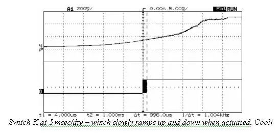
Figure. The Conductive Rubber Switch (K) Has a Smooth Voltage Rise, but Causes Severe Oscillation at the Digital End Due to Slowly Crossing the Threshold Region
Therefore, we must recognize that the “bounce” we deal with is not just the mechanical bouncing of physical contacts but also includes digital logic misjudgments caused by poor analog signal characteristics (such as slow edges and hovering near the threshold). The effects produced by these two phenomena at the system level are the same and require debouncing to resolve.This also warns us that simple debouncing algorithms, such as “considering it stable if two consecutive readings are the same,” may not be reliable!!!
Throughout the entire time window of the bounce, what does the signal look like? Each bounce can be said to be unique! Some bounces manifest as a series of high-frequency noise before finally stabilizing. Others produce a series of logical pulses that can cause simple debouncing algorithms to fail.
Taking the previously mentioned switch E, which has a bounce duration of up to 157ms, as an example. In one test, it first stabilized outputting logic “1” for up to 81ms, then suddenly switched to a perfect logic “0” and maintained it for 42ms before finally stabilizing at the correct logic “1” state.Almost any debouncing algorithm based on simple delays or counts would be deceived by this “stabilize then bounce back” behavior!!!
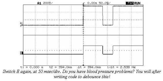
Figure. Switch E Exhibits Complex Behavior of First Stabilizing at High Level for a Long Time, Then Jumping to Low Level, and Finally Stabilizing
Switch G’s behavior reveals another risk. In several tests, it produces a narrow pulse of “1” lasting only a few microseconds before finally stabilizing to logic “1”, followed by a stable “0” for over 2ms. If this switch input is connected to an interrupt pin, that momentary narrow pulse is enough to trigger the interrupt service routine (ISR). However, when the ISR starts executing and reads the pin state, it finds the input is stable low, leading to a misjudgment.
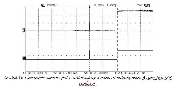
Figure. After Switch G Produces a Narrow Pulse Sufficient to Trigger an Interrupt, It Enters a Stable Low Level for Up to 2ms Before Finally Changing to High Level
A high-quality micro switch (Sample O), although its total bounce duration never exceeds 1.18ms, exhibits a bounce process consisting of a series of clear pulses of 0s and 1s with widths on the order of tens of microseconds. This signal pattern poses a significant challenge for algorithms that merely look for “N consecutive stable readings,” as the signal may briefly appear stable in both logical states before the bounce ends.
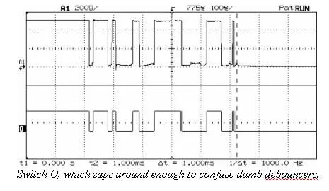
Figure. The Bounce of Switch O Consists of a Series of Clear Pulses That Are Difficult to Filter Out Using Simple Counting Methods
These cases fully illustrate that designing a truly reliable debouncing system must consider the diversity and complexity of bounce phenomena and cannot rely on overly idealized models.
Due to the aforementioned drawbacks, more complex software debouncing algorithms are often required. However, this introduces new issues: software complexity; a complex debouncing program increases the difficulty of code maintenance. It is essential to conduct actual bounce characteristic tests on pre-selected switches when using software debouncing algorithms. Purchasing at least three samples for measurement can provide a more reliable basis for assessing their statistical characteristics, thus determining whether the bounce duration of mechanical contacts is consistent.
For hardware debouncing solutions, the core advantages lie in “real-time” and “independence”: it purifies the signal before it enters the system, does not consume any CPU resources, and its response is instantaneous. For certain high-speed or high-reliability applications, hardware debouncing remains an indispensable choice.
There are two classic hardware debouncing circuits: the SR latch scheme and the RC network scheme.
The SR latch (Set-Reset Latch) is one of the most thorough and reliable hardware methods for solving switch bounce. Its basic circuit is shown in the figure below, consisting of two cross-coupled NAND gates.
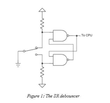
Figure. Classic SR Latch Debouncing Circuit
The key to this circuit design is that it requires a double-throw switch, which is a switch with normally open (NO) and normally closed (NC) contacts. Two pull-up resistors ensure that the inputs of the NAND gates are high when the switch is floating.
Its working principle is as follows:
1. Initial State: As shown in the figure, when the switch closes to the upper contact, the input A of the upper NAND gate is pulled low to ground (logic 0). Regardless of the level at point B, according to the logic characteristics of the NAND gate, its output Q will be high (logic 1). This high level Q, along with the high level provided by the lower pull-up resistor, serves as the input to the lower NAND gate, making its output /Q low (logic 0). This low level /Q then feeds back to the B input of the upper NAND gate, further locking the current state. At this point, the output (Q, /Q) is (1, 0).2. Switching Process: When the user toggles the switch from the upper contact to the lower contact, there will be a brief “floating” phase where both contacts are not connected to the common terminal. During this period, due to the presence of the two pull-up resistors, both inputs A and B are high. However, since the output /Q of the lower NAND gate (logic 0) feeds back to the B input of the upper NAND gate, even if A becomes high, the output Q remains 1. Therefore, the entire latch state is maintained, and the output remains unchanged.3. Bounce Occurs: When the common terminal of the switch contacts the lower contact, bouncing may occur. At the moment of contact, the input of the lower NAND gate is pulled low, causing its output /Q to become high. This high level, along with the high level at the A input (which is now floating), causes the output Q of the upper NAND gate to become low. This low level Q feeds back to the input of the lower NAND gate, locking the high level state of /Q. As long as the switch does not bounce far enough to re-contact the upper contact (which is physically almost impossible), the circuit state will stabilize at (Q, /Q) = (0, 1), thus outputting a clean, bounce-free level transition.
The output of the SR latch scheme is absolutely clean because it uses state feedback to “remember” the first valid contact of the switch and ignores subsequent bounces.
Although the SR latch scheme is highly effective, double-throw switches are larger and more expensive than ordinary single-throw switches, and many buttons cannot achieve a double-throw structure, so it is not commonly used in practical engineering.
RC Network-Based Debouncing Circuit
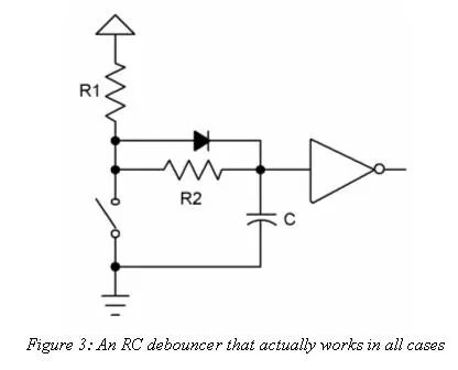
For designs that are more sensitive to cost and size, especially in cases using single-throw switches, the RC (resistor-capacitor) network is the most common hardware debouncing solution. It utilizes the characteristic that capacitor voltage cannot change instantaneously to smooth out voltage jumps caused by switch bounce.
An optimized RC debouncing circuit is shown in the figure below.
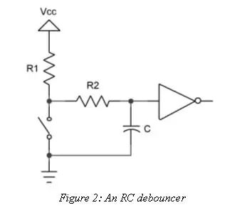
Figure. RC Debouncing Circuit with Input Protection Resistor R2
Analysis of Circuit Working Principle:
1. Switch Open (Charging Process): When the switch S1 is open, the power supply +V charges the capacitor C through resistors R1 and R2. The voltage across the capacitor Vc will rise slowly according to an exponential law. During this time, the switch contacts may briefly close due to bouncing, but this will only temporarily pull Vc down, and once the contacts bounce open again, the charging process will continue. As long as the RC time constant is chosen appropriately, during the entire bounce period, the voltage Vc will not rise to the threshold recognized as “high level” by the logic gate. After the bounce ends, Vc will stabilize and charge up to +V level.2. Switch Closed (Discharging Process): When the switch S1 is closed, the capacitor C discharges through resistor R2. The voltage Vc will slowly decrease. Bouncing may cause the contacts to momentarily open, during which the power supply will attempt to charge the capacitor through R1 + R2, slowing down the discharge process and helping to maintain Vc at a higher level during the bounce. Similarly, as long as the RC parameters are appropriate, Vc will not drop below the threshold for logic “low level” before the bounce ends.
The Key Role of Resistor R2
Many textbooks omit R2 in RC debouncing circuits, allowing the capacitor to discharge directly through the switch when closed. This is a dangerous design. When a charged capacitor closes through an ideal switch, it generates an instantaneous, theoretically infinite discharge current (I = C * dV/dt). This massive surge current can not only damage the metal contacts of the switch, shortening its lifespan, but the parasitic inductance (ESL) on the leads and PCB traces can form an LC oscillation circuit with the capacitor C, producing ringing that exceeds the power supply voltage, potentially causing EMI issues.
Resistor R2 plays two important roles here:
Limiting Discharge Current: It limits the peak current during capacitor discharge, protecting the switch contacts.Ensuring Slow Discharge: It, along with capacitor C, determines the discharge time constant, ensuring that even during bouncing, Vc can slowly decrease, effectively filtering out the bounce.
Schmitt Trigger – An Indispensable Partner for RC Debouncing
The output of the RC network is a slowly changing analog voltage. As mentioned above, if such a slowly changing signal is directly input to standard digital logic gates or microcontroller pins, when the voltage slowly crosses the uncertain region of the logic threshold, it can lead to logic oscillations at the input stage, producing a series of high-frequency noise, exacerbating the problem.
Therefore, the output of the RC debouncing circuit must be connected to a device with a Schmitt trigger input.
A Schmitt trigger is a comparator with “hysteresis” characteristics. It has two different switching thresholds: one for the rising edge “high threshold” (Vth+), and one for the falling edge “low threshold” (Vth-).
- When the input voltage rises from low to high, the output will only switch to high when it exceeds Vth+.
- When the input voltage falls from high to low, the output will only switch to low when it drops below Vth-.
Within the voltage range between Vth- and Vth+, the output state remains unchanged. This hysteresis characteristic can perfectly “purify” the slowly changing signal output from the RC network. Even if the signal has small noise fluctuations near the threshold, as long as the fluctuation range does not cross the difference between the two thresholds (i.e., the hysteresis voltage), the output will remain stable, resulting in a clean, bounce-free digital signal. Common chips like 74HC14/74AHCT14 are popular choices that integrate six Schmitt trigger inverters.
Design Guidelines: Never directly connect the output of an RC filtering network to the I/O pins of ordinary microprocessors or logic devices unless the pin is explicitly marked as having Schmitt trigger input characteristics.
Parameter Design for RC Debouncing Circuits
The core of RC circuit design is selecting appropriate R and C values to ensure that during the estimated maximum bounce time, the capacitor voltage does not cross the logic threshold of the Schmitt trigger.
Based on experimental data, most switches have bounce durations far below 10ms. To allow for sufficient margin, we can choose a debouncing time of 20ms (T_debounce).
1. Discharge Process (Switch Closed)
The voltage equation for capacitor discharge is:
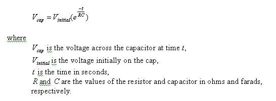
Where <span>V_initial</span> is the initial voltage (here Vcc, e.g., 5V). We need to ensure that at <span>t = T_debounce</span>, <span>Vcap</span> is still above the falling edge threshold of the Schmitt trigger <span>Vth-</span>.
Rearranging the time constant formula to solve for R (the cost and size differences of capacitors are significant, so it is best to choose a C value first and then calculate R) gives:
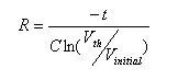
R * C = -t / ln(<span>Vth</span> / V_initial)
Taking 74AHCT14 as an example, its worst-case <span>Vth-</span> (referred to as V_T- in the datasheet) is approximately 1.7V under 5V supply.
Substituting <span>t = 20ms</span>, <span>Vth</span><span>= 1.7V</span>, <span>V_initial = 5V</span>:
R * C = -0.02 / ln(1.7 / 5) = -0.02 / (-1.078) ≈ 0.0185
Typically, we first choose a common capacitor value and then calculate the resistor. Choosing <span>C = 0.1µF</span>, which is a common and inexpensive value. Solving for the condition when the switch just closes, the capacitor discharges through R2. If the power supply is 5 volts (thus Vinitial is 5), then R2 is 185K. Of course, you won’t actually find a resistor of that value, so use 180K.
However, this analysis ignores the input leakage current of the gate. CMOS devices like 74AHCT14 leak about one microamp of current from the input. That 180K resistor would bias the input to 0.18 volts, which is very close to the optimal switching point of 0.5 volts for the gate, which is concerning. Changing C to 1 µF, R2 is now 18K.
R1 + R2 controls the capacitor’s charging time, thus setting the debouncing period when the switch is open. The charging equation is:
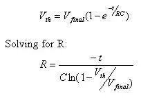
<span>Vth = V_final * (1 - e^(-t / ((R1 + R2) * C)))</span> Where <span>V_final</span> is the final voltage (Vcc, 5V). We need to ensure that at <span>t = T_debounce</span>, <span>Vth</span> is still below the rising edge threshold of the Schmitt trigger <span>Vth+</span>.
For 74AHCT14, its worst-case <span>Vth+</span> (referred to as V_T+ in the datasheet) is approximately 0.9V (note that this is an inverter, so the input is low, and the output is high).
Rearranging the formula to solve for (R1 + R2) * C:
<span>(R1 + R2) * C = -t / ln(1 - Vth / V_final)</span>
Substituting <span>t = 20ms</span>, <span>Vth = 0.9V</span>, <span>V_final = 5V</span>:
<span>(R1 + R2) * C = -0.02 / ln(1 - 0.9 / 5) = -0.02 / ln(0.82) = -0.02 / (-0.198) ≈ 0.101</span>
<span>R1 + R2 = 0.101 / (1 * 10^-6) = 101kΩ</span>
Knowing R2 is approximately 18kΩ, then<span>R1 = 101kΩ - 18kΩ = 83kΩ</span>. Choosing a resistor with a nominal value of 82kΩ will suffice.
Design Considerations:
-
Input Leakage Current: CMOS devices (like 74AHCT14) typically have an input leakage current of around 1µA. This current flowing through R1 + R2 will produce a small voltage drop. If the resistance value is too high (e.g., above several hundred kΩ), this voltage drop may affect the logic level judgment. Therefore, when selecting C, it should not be too small to avoid calculating an excessively large R value.
<span>C = 1µF</span>and tens of kΩ resistors are a relatively balanced choice. -
Component Tolerance: The tolerance of ordinary resistors is ±5%, while the tolerance range for capacitors can be larger, especially for electrolytic capacitors (up to +80%/-20%). In design, the worst-case component values and logic thresholds should be used for calculations to ensure design reliability.
Other Considerations in Hardware Design
-
Avoid Directly Connecting to Clocks or Interrupts: Never connect untreated switch signals to the clock input of a flip-flop or the interrupt pin of a microprocessor. The high-frequency noise and narrow pulses in the bouncing signal can easily violate the timing requirements of the flip-flop’s minimum pulse width, setup time, and hold time, leading to metastability or incorrect latching. Most MCU datasheets do not detail the electrical characteristics of interrupt pins, but they are usually connected to some internal timing logic unit, so there is a similar risk.
-
Dedicated Debouncing ICs: There are some dedicated debouncing chips on the market, such as the MC14490, which integrate multiple debouncing units. These chips are easy to use and reliable in performance, but they are relatively expensive. In many modern designs, using a cheap microcontroller (like the PIC or AVR Tiny series) to implement software debouncing may result in a total cost lower than using a dedicated debouncing IC.
-
Unused Logic Inputs: This is a general rule in digital circuit design: any unused logic gate inputs must not be left floating. They must be connected to Vcc or ground to prevent the input from floating near the logic threshold due to interference such as static electricity, leading to unnecessary power consumption and logic oscillation.
Firmware Debouncing Solutions
As MCU performance improves and costs decrease, using firmware to implement switch debouncing has become the preferred choice for the vast majority of applications. Software solutions not only eliminate the need for external hardware components, reducing BOM costs and PCB area, but also provide unparalleled flexibility, allowing easy adjustments to debouncing parameters and even implementing different debouncing strategies for different switches.
Basic Principles of Firmware Debouncing
Before writing code, we need to establish a clear design strategy. An excellent debouncing firmware should not only handle mechanical bounce but also cope with external noise such as electromagnetic interference (EMI), while ensuring system responsiveness and effective resource utilization.
-
Handling EMI Noise: The leads on the circuit board, especially the cables connected to external switches, act like antennas and can pick up electromagnetic noise from the environment. This noise may manifest as brief voltage spikes, sufficient to cause erroneous level transitions at the MCU’s input pins, producing effects similar to mechanical bounce. A robust debouncing algorithm must be able to filter out both types of interference simultaneously.
-
Minimizing CPU Overhead: Debouncing is a low-priority background task in the system. While waiting for the switch state to stabilize, blocking delays through
<span>for</span>loops or<span>while</span>loops should never be used. This “busy waiting” wastes CPU cycles and may even affect more critical real-time tasks in the system. All reliable debouncing algorithms should operate in a non-blocking manner based on timer interrupts or the scheduling mechanism of the operating system. -
Using Regular I/O Instead of Interrupt Pins: As mentioned above, untreated switch signals should not be connected to the interrupt pins of the MCU. The chaotic signal sequences generated by bouncing may violate the timing requirements of the internal flip-flops. Therefore, switches should be connected to regular GPIO pins, and the software should poll them at a fixed frequency, triggering the corresponding logical actions only after the state stabilizes.
-
Avoid Synchronous Sampling: The choice of sampling rate should avoid synchronizing with periodic noise sources that may exist in the environment. For example, in a mains environment, sampling at integer multiples of 50Hz or 60Hz should be avoided to prevent power frequency interference from being misidentified as switch actions. In automotive applications, it may even be necessary to avoid sampling rates related to engine or steering column vibration frequencies.
-
Ensuring Fast Response: User experience is crucial. The delay from when a user presses a button to when the system provides feedback must be as short as possible. Experiments show that delays below 50ms are perceived as almost “instantaneous” by humans, while delays exceeding 100ms create a noticeable “lag.” Therefore, our debouncing algorithm should strive to confirm user actions as quickly as possible while ensuring reliability.
Timer and State Machine-Based Debouncing Algorithm
This is one of the most classic and universal debouncing methods, abstracting the debouncing process into a time-based state machine. The algorithm is driven by a periodically called function (usually triggered by a timer interrupt).
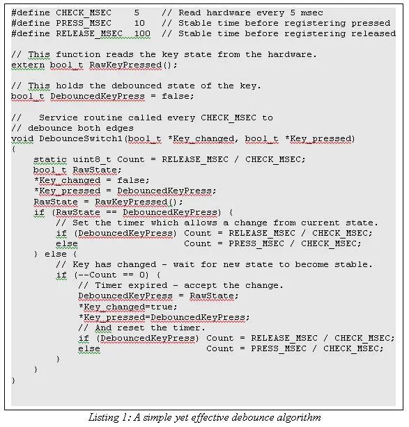
Algorithm Analysis:
-
The function
<span>DebounceSwitch1()</span>must be called at fixed time intervals<span>CHECK_MSEC</span>(e.g., 5ms). -
It uses static variables
<span>count</span>and<span>button_state</span>to save the state between two calls. -
When a change in pin level is detected, it is considered that a bounce period may have begun, at which point
<span>button_state</span>is updated to the current state, and<span>count</span>is reset. -
If the pin level remains unchanged, then
<span>count</span>continues to increase. -
By converting the count value to a stable duration through
<span>count * CHECK_MSEC</span>, when this time exceeds the preset threshold (for pressing<span>PRESS_MSEC</span>or releasing<span>RELEASE_MSEC</span>), the switch state is finally confirmed (<span>Key_Pressed</span>). -
<span>Key_Changed</span>flag is used to notify the main program of a valid state change, facilitating event-driven logic implementation.
The greatest advantage of this algorithm is that it is based on time rather than counts, making it very robust and easy to maintain. Regardless of changes in CPU clock frequency or compiler, the debouncing delay is explicitly determined by the macro definitions <span>PRESS_MSEC</span> and <span>RELEASE_MSEC</span>. Additionally, setting different debouncing times for pressing and releasing provides extra flexibility, such as allowing for a quick response to user presses (smaller <span>PRESS_MSEC</span>) while providing stronger protection against EMI interference after release (larger <span>RELEASE_MSEC</span>).
Shift Register Debouncing Algorithm
This is a more streamlined and efficient algorithm, particularly suitable for resource-constrained MCUs or situations requiring translation into assembly language. Its core idea is to use an integer variable as a “shift register” to record the recent N samples of the pin.
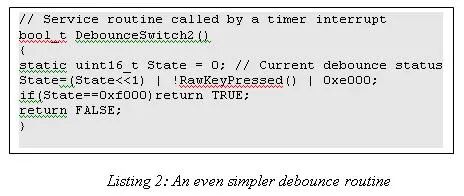
Algorithm Analysis:
-
Similarly, this function also needs to be periodically called by a timer.
-
Static variable
<span>state_history</span>represents the result of each sample. Each time it is called, the latest sample value (0 or 1) is shifted into the lowest bit of the variable. -
By comparing with a specific mask (e.g.,
<span>0xFFF0</span>), we can determine whether the switch has maintained a stable state in the most recent N samples. For example,<span>state_history == 0xFFF0</span>means that after experiencing a period of uncertainty (high bits are 1), the last four sample values were all 0. This accurately captures the transition from bouncing/releasing to stable pressing. -
This method cleverly compresses historical information into a single variable, allowing for efficient judgment through bitwise operations. It not only filters out bounce but also naturally implements edge detection, returning
<span>TRUE</span>only at the moment of stable state transition.
This algorithm is very efficient, with almost no branching and fixed execution time, making it very suitable for hardware logic implementation in FPGAs or ASICs.
Processing Multiple Switches in Parallel
When needing to process an entire port (e.g., 8 switches), applying the above algorithm to each one individually is inefficient. We can incorporate parallel thinking into the debouncing algorithm to handle multiple inputs simultaneously.
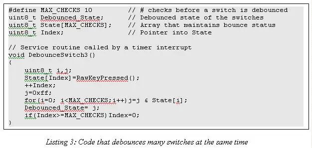
Algorithm Analysis:
- This algorithm maintains a circular queue `State` to store the most recent `DEBOUNCE_SAMPLES` readings for the entire port.
- The core idea is: If a switch (corresponding to a bit) has maintained the same state in all recent samples, then it is stable.
- By performing bitwise AND (`all_and`) and bitwise OR (`all_or`) on all bytes in the queue, we can determine which bits are stable. If a bit has the same value in both `all_and` and `all_or`, it indicates that the bit has not changed throughout the entire historical window.
- `stable_mask` calculates the mask of all stable bits.
- Finally, only the stable bits are used to update the final `Debounced_State`, while unstable bits retain their last stable state. To detect state changes, simply XOR the current `Debounced_State` with the previous value.
This algorithm efficiently implements high-performance parallel debouncing for the entire port with minimal code, making it an ideal choice for applications like matrix keyboards.
Key Points of Software Debouncing
All reliable software debouncing algorithms share a common feature: they rely on a periodic, timer-driven sampling mechanism.
-
Sampling Rate: To achieve good responsiveness without overloading the CPU, a 1ms to 5ms timer interrupt (i.e., sampling period) is a relatively ideal choice.
-
Debouncing Time: Combining experimental data (most bounces end within 10ms) and user experience (responses greater than 50ms are perceived by humans), a 20ms to 50ms debouncing confirmation time is reasonable. This means that the switch state must be continuously stable for 20ms to 50ms to be considered a valid change.
Industrial-Grade High-Reliability Input Circuit Design
A robust industrial-grade input circuit is designed not only to eliminate bounce but also to effectively isolate the external harsh electromagnetic environment from the fragile internal digital control core and filter out various high-frequency noise. The figure below shows a classic circuit that comprehensively utilizes opto-isolation, RC filtering, and Schmitt triggering to accomplish this task.
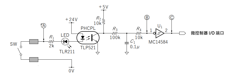
This circuit mainly consists of three stages: opto-isolator, RC low-pass filter (integrating circuit), and Schmitt trigger.
(1) Opto-Isolator: Achieving Electrical Isolation and Noise Blocking
The first stage of the circuit is the opto-isolator. Its core function is electrical isolation, which completely disconnects the ground of the input side (external) circuit from the output side (internal) circuit during signal transmission. This brings two major benefits:
- Blocking Common-Mode Noise: In industrial environments, there may be potential differences between the ground lines of different devices (ground loops), or the entire ground network may be subjected to strong noise interference. The opto-isolator transmits signals through light, physically cutting off the ground connection, effectively preventing these common-mode noises from being conducted to the microcontroller side through the ground.
- Protecting Core Circuits: External input cables may be subjected to high-voltage surges or static shocks. The insulation layer of the opto-isolator can withstand transient high voltages of several thousand volts, thus protecting the low-voltage microcontroller from damage.
To further enhance noise immunity, the input side of this circuit (LED driving side) typically uses a voltage higher than the microcontroller logic level, such as 12V or 24V. A higher driving voltage means a higher signal-to-noise ratio (SNR) under constant noise amplitude. Additionally, to ensure reliable LED illumination, the driving current should also be set relatively high (e.g., 10-20mA). This “strong signal” design not only resists noise but also effectively overcomes the increased contact resistance of switch contacts due to long-term use or environmental oxidation, ensuring long-term reliability of the contact.
(2) RC Low-Pass Filter: Filtering Out Bounce and High-Frequency Noise
After the signal is isolated by the opto-isolator, it enters the RC debouncing circuit composed of resistor R and capacitor C, which also functions to filter out high-frequency components.
The selection of the RC time constant (τ = R × C) is crucial. It must be greater than the expected maximum bounce time but less than the minimum signal response time allowed by the system. In general-purpose switch input scenarios where high-speed response is not required, the time constant can be increased to achieve stronger anti-interference performance.
(3) Schmitt Trigger: Waveform Shaping and Logic Level Restoration
Although the signal after RC filtering eliminates bounce, its edges become very smooth. If such a “slow edge” signal is directly sent to standard digital logic gates, it may cause two problems: first, the logic gate may produce multiple output transitions (oscillations) when the input voltage crosses its threshold region due to minor noise; second, the input level being in the uncertain region for an extended period may cause the internal CMOS transistors of the logic gate to conduct simultaneously, increasing power consumption or even damaging the device.
The Schmitt trigger is the ideal device to solve this problem. It can shape slowly changing input signals into standard digital signals with steep edges, ensuring that subsequent digital circuits can process them stably and reliably.
References
[1] A very strong website: https://www.ganssle.com/debouncing.htm