Overview
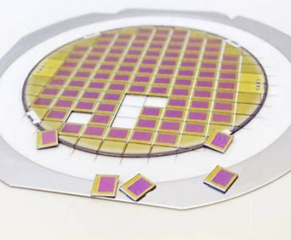
Integrated circuits are composed of chips (die) cut from silicon wafers (wafer). Each wafer can yield hundreds of chips.
ASIC stands for Application Specific Integrated Circuit, which is designed for specific applications, unlike general-purpose memory, microprocessors, etc. There are several types of ASICs:
-
Full-Custom ASIC: This type of ASIC is completely manually designed, without using pre-designed logic gates, but rather drawing the chip layout by hand.
-
Standard Cell ASIC: This type of ASIC uses pre-designed logic gates, such as AND, NOR, etc., to construct circuits. These logic gates are referred to as standard cells. The advantage of Standard Cell ASICs is that designers can save time, money, and risk because the standard cell library has already been designed and tested. Each standard cell is designed using a full-custom approach and can be optimized individually.
When designing an ASIC, several goals must be balanced:
-
Speed: Refers to the clock frequency and response time of the chip, affecting its performance and efficiency.
-
Area: Refers to the silicon wafer area occupied by the chip, affecting its cost and yield.
-
Power: Refers to the energy consumed by the chip during operation, affecting its reliability and heat dissipation.
-
Time to Market: Refers to the time required from design start to product launch, affecting the chip’s competitiveness and market share.
To achieve these goals, designers need to be familiar with CMOS technology, which is the technique for manufacturing chips using Complementary Metal Oxide Semiconductor.
CMOS Technology
1.1 CMOS Technology
CMOS technology is currently the most widely used chip manufacturing technology, utilizing Complementary Metal Oxide Semiconductor to construct circuits. CMOS circuits are composed of two types of MOSFET transistors: NMOS and PMOS.
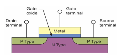
1.2 MOSFET Transistor
MOSFET stands for Metal Oxide Semiconductor Field Effect Transistor, which is a voltage-controlled switching device and a fundamental unit in digital integrated circuit design. The structure and working principle of a MOSFET are shown in the following figures.
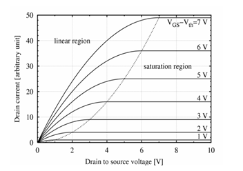
CMOS technology uses both NMOS and PMOS MOSFETs to achieve high-density, complex digital integrated circuits, primarily used for signal processing. The advantages of CMOS technology include low power consumption, high speed, and ease of integration. In digital ICs, MOSFETs can be viewed as simple switches. For example, a CMOS inverter requires only one PMOS and one NMOS transistor.
-
When the input is logic “0”, the PMOS is on, the NMOS is off, the output load capacitance is charged, and the output is logic “1”.
-
When the input is logic “1”, the PMOS is off, the NMOS is on, the output load capacitance is discharged, and the output is logic “0”.
The output load capacitance of a logic gate consists of intrinsic capacitance and external capacitance (such as wiring, fan-out, etc.). The carriers in PMOS and NMOS are holes and electrons, respectively. Since the mobility of electrons is more than twice that of holes, this leads to asymmetry in the output rise and fall times.
To balance this difference, the width-to-length ratio (W/L) of PMOS is typically made larger than that of NMOS. This allows PMOS and NMOS to have similar drive strengths.
In the standard cell library, the length L of the transistors is generally fixed, while the width W is adjusted according to the driving requirements of different gates.
1.3 Power Consumption of CMOS Integrated Circuits
The power consumption of CMOS integrated circuits mainly has the following three sources:
-
Dynamic Power: Generated due to the charging and discharging of the circuit load capacitance during switching. Given frequency f, dynamic power is: load capacitance * Vdd * Vdd * f
-
Short-Circuit Power: Generated due to the simultaneous conduction of PMOS and NMOS during switching, forming a short-circuit path.
-
Static Power: Generated due to leakage current in the transistors.
1.4 CMOS Transmission Gate
Connecting PMOS and NMOS in parallel forms a transmission gate. The transmission gate can pass the input signal to the output.
1.5 Sequential Elements
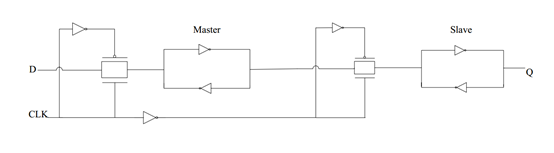
In CMOS, logic values can be stored through feedback loops, and such elements are called sequential elements. The simplest sequential element is two inverters connected to each other. Based on this structure, there are two basic types of sequential elements:
1. Latch: A latch is formed by adding a transmission gate between two inverters to control data input and output.
-
When the control signal of the transmission gate is logic “1”, the transmission gate is open, and the input signal “D” can be passed to the output.
-
When the control signal is logic “0”, the transmission gate is closed, and the output retains its previous value.
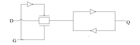
2. Flip-Flop: A flip-flop is formed by connecting two latches in series. The first latch is called the Master Latch, and the second latch is called the Slave Latch.
In this case, the control signal for the transmission gate is the clock signal. The clock signal is inverted and sent to the transmission gate of the slave latch.
-
When the clock signal is high, the transmission gate of the master latch is open, and the input signal “D” can be latched by the two inverters. Meanwhile, since the clock signal is inverted, the transmission gate of the slave latch is closed, and the output signal “Q” retains its previous value.
-
When the clock signal is low, the transmission gate of the slave latch is open, and the output signal “Q” is updated to the value latched by the master latch. At this point, the output signal “Q” is independent of the changes in the input signal “D”.
Since the flip-flop only updates data on the rising edge of the clock signal, this type of flip-flop is called a positive edge-triggered flip-flop. If the flip-flop only updates data on the falling edge of the clock signal, it is called a negative edge-triggered flip-flop.
Chip Design Process
To design a chip, a clear design goal and functional requirements (Idea) must first be established.
In the ASIC design process, this Idea will continuously transform into different representations.
The first step in the ASIC design process is to write the Idea into a detailed specification document (Specifications). The specification document includes:
-
The design goals and constraints.
-
The functional description of the design.
-
The performance metrics of the design, such as speed and power consumption.
-
The area estimation of the design.
-
The choice of manufacturing process and design methodology.
Traditionally, the ASIC design process is as follows:
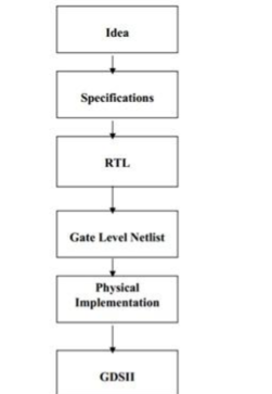
1. Provide the structural and functional decomposition of the design (Structural and Functional Description). This means determining what kind of design architecture to use, such as RISC/CISC, ALU, pipelining, etc., and dividing the entire system into several sub-modules. The functions of each sub-module must also be clearly defined in the specification document.
2. After determining the system hierarchy, the design’s functionality must be implemented using specific logic elements. This step is called RTL-level logic design (Register Transfer Level). RTL design is typically written in hardware description languages (Verilog, VHDL). Hardware description language (HDL) is a language used to describe digital systems and can represent logic gates, microprocessors, memory, flip-flops, and any level of hardware. At this stage, functional verification of the design must be performed to ensure it meets the requirements of the specification document.
3. Functional verification
4. Logic synthesis, using tools like Design Compiler (Synopsys), Genus (Cadence), etc., to convert RTL code into an optimized gate-level netlist (Gate Level Netlist). Synthesis tools require RTL code and a standard cell library (Standard cell library) as input and output a gate-level netlist. The standard cell library is a collection of commonly used basic logic modules in integrated circuit design. During logic synthesis, the synthesis tool must consider various constraints (Constraints), such as timing, area, testability, and power consumption. The synthesis tool will seek the best implementation scheme that meets the constraints based on different optimization strategies and cost functions. After logic synthesis is completed, a gate-level netlist containing only structural information and no behavioral information is obtained.
5. Perform functional verification on the gate-level netlist to check for consistency with the RTL code.
6. Physical implementation of the gate-level netlist. This step maps the gate-level netlist to specific locations and wiring on the chip. Physical implementation must consider manufacturing process constraints on layout and routing, such as DRC rules. The physical implementation steps include three sub-steps: Floor planning -> Placement -> Routing. The output of physical implementation is a GDSII file, which is the required file format for chip manufacturing. Physical implementation can be completed using software like IC Compiler (Synopsys), Innovus (Cadence), etc.
7. Perform physical verification to check compliance with DRC rules, LVS rules, etc.
8. Timing analysis. For any design with specific clock frequency requirements, timing analysis (timing analysis) must be performed. We need to check whether the design meets the timing requirements specified in the specification document. This is done using static timing analysis (Static Timing Analysis) tools, such as Primetime (Synopsys). It checks all timing paths in the design to verify whether there are timing violations (timing violations). For example: setup time, hold time, etc.
9. After both physical implementation and timing analysis pass, the design can be delivered to the manufacturing plant for fabrication. After manufacturing, the chip will be cut, packaged, and tested.
Finally, it is worth considering whether we must strictly adhere to this waterfall development process??? Can we shift the process left as much as possible?