Author: Wei Die, Hu Zhongyang
Originally published by “Digital Enterprises”
In recent years, with the rapid development of digital technology and artificial intelligence, the application fields of chips have been continuously expanding, and their importance in global economic and social development is increasing day by day. The demand for the global chip market continues to grow, and the structure of the chip industry chain from design, manufacturing to packaging and testing is rapidly changing, with the industry chain structure constantly optimizing. This article will provide a brief analysis of the global and Chinese chip industry chain, for the reference of a wide range of readers.
Interpretation of the Chip Industry Chain
The Complete Chip Industry Chain
The complete chip industry chain mainly includes key links such as chip design, manufacturing, and packaging testing. In addition, related supporting industries, including chip manufacturing equipment and key materials, have also emerged. According to the division of upstream and downstream industries, the chip industry chain can be simply divided into: upstream includes EDA software, materials, and equipment required for chip manufacturing; midstream includes the chip design and manufacturing process, including chip design, chip manufacturing, and packaging testing; downstream is widely applied in communication equipment, artificial intelligence, automotive electronics, consumer electronics, the Internet of Things, industry, medical, military, and other fields. As shown in Figure 1:
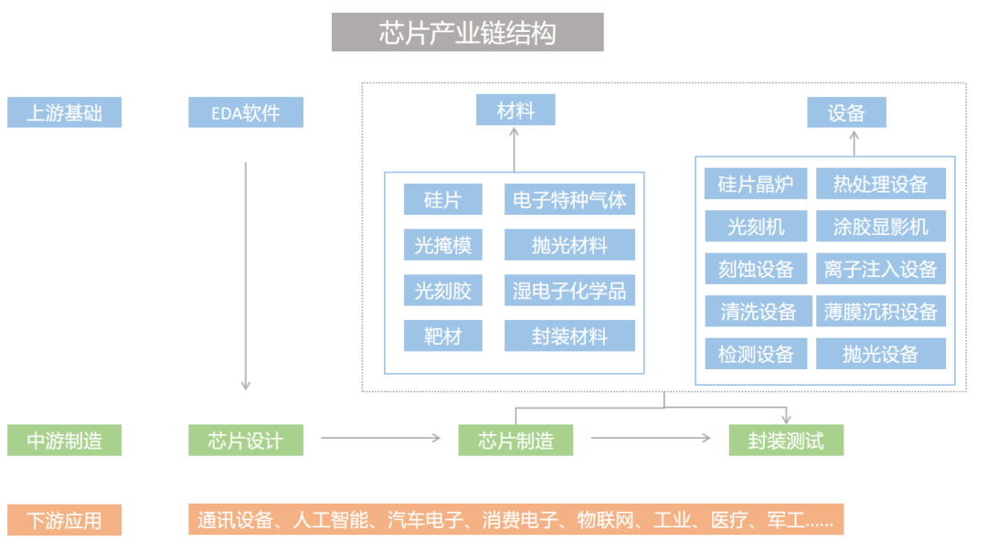
Figure 1 Chip Industry Chain Structure Analysis
Among them, EDA software is the core tool for chip design, supporting the chip design and manufacturing process, serving as the carrier of chip design methodology, and is also the link and bridge connecting the design and manufacturing stages, positioned upstream in the chip industry chain.
A complete chip design and manufacturing process mainly includes three stages: process platform development, chip design, and chip manufacturing. The process platform development stage is mainly led by wafer fabs. After completing the design of semiconductor devices and manufacturing processes, they establish models of semiconductor devices and provide them to chip design companies through PDK (Process Design Kit) or by establishing IP and standard cell libraries. The chip design stage is mainly led by chip design companies, which conduct circuit design, simulation verification, and physical implementation based on the PDK or IP and standard cell libraries provided by the wafer fabs. The chip manufacturing stage is mainly carried out by wafer fabs based on the design files after physical implementation.
All three main stages of design and manufacturing require corresponding EDA tools for support, including manufacturing EDA tools for the process platform development and chip manufacturing stages, and design EDA tools supporting the chip design stage.
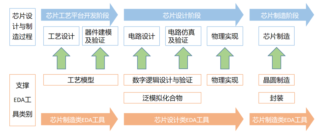
Figure 2 The Supporting Role of EDA Tools in Chip Design and Manufacturing Stages
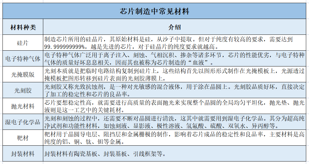
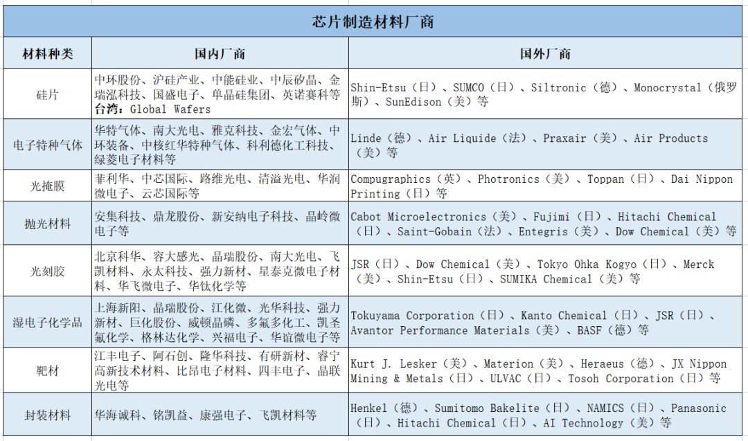
Chip manufacturing equipment and materials are two other important supporting links located upstream in the chip industry chain.We can simply divide the chip manufacturing process into eight steps: wafer processing, oxidation, photolithography, etching, thin film deposition, interconnection, testing, and packaging. The required equipment includes silicon wafer furnaces, thermal processing equipment, photolithography machines, coating and developing machines, etching equipment, ion implantation equipment, cleaning equipment, thin film deposition equipment, inspection equipment, polishing equipment, etc. In addition, the main materials used in the chip manufacturing process include silicon wafers, specialty electronic gases, photomasks, photoresists, polishing materials, high-purity wet electronic chemicals, targets, packaging materials [1], etc. The introduction of various equipment and materials is shown in Tables 1 and 2 below.
Table 1 Common Equipment in Chip Manufacturing
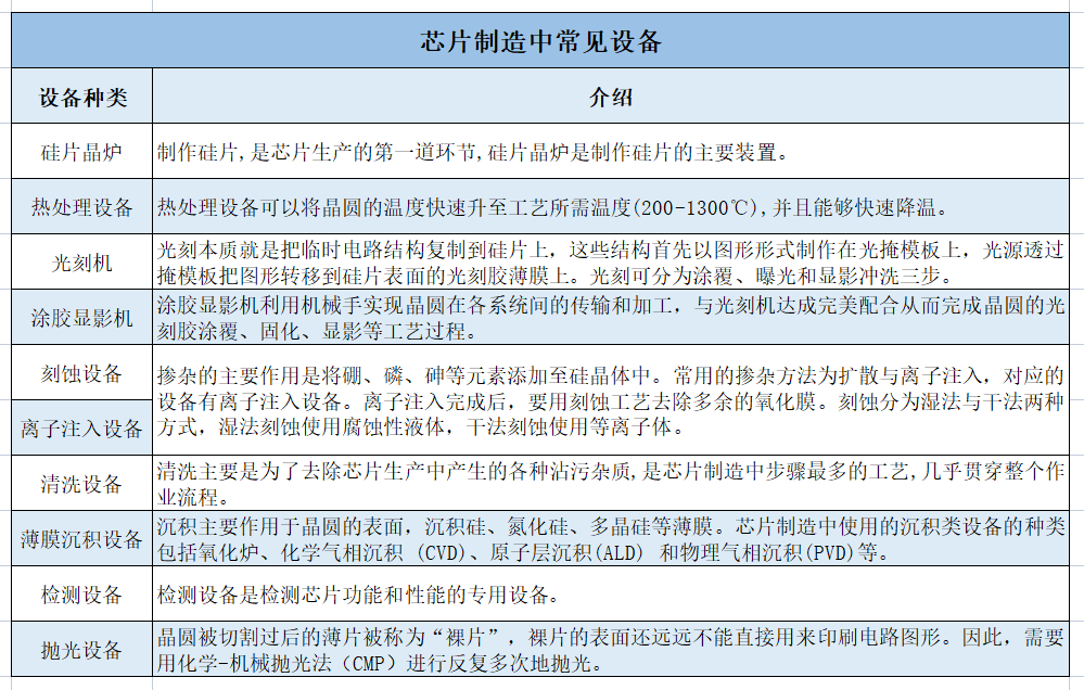
Table 2 Common Materials in Chip Manufacturing
Note: We have summarized three generations of semiconductor materials based on the classification dimension of semiconductor material types. Among them, silicon and germanium are first-generation materials; gallium arsenide and indium phosphide are second-generation materials; silicon carbide and gallium nitride are third-generation materials. Silicon is currently the most widely used chip material, and most common chips are made from silicon materials. Here, we mainly summarize common materials in chip manufacturing, so only silicon wafers are included.
Chip design is located in the midstream of the chip industry chain, and the functions that the chip can achieve mainly depend on the initial overall design of the chip. It converts the design of systems, logic, and performance into specific physical layouts, including key steps such as specification formulation, RTL (Register Transfer Level) code implementation, coding checks and analysis, functional verification, logic synthesis, layout routing, static timing analysis, physical verification, power analysis, and timing simulation.
Packaging testing is the third specialized link in the midstream of the chip industry chain. The main role of chip packaging is to provide a sturdy and durable protective shell for small, precise, and easily damaged bare chips while connecting the densely packed micro-signal contacts on the bare chip to the larger electrical signal pins or solder points outside the package, so that the chip can be easily soldered into electronic components. Chip testing usually includes two steps: functional testing and performance testing. Functional testing is the process of checking whether the chip’s functions are normal, typically including checking the chip’s inputs, outputs, and whether their logical connections are correct. Performance testing ensures that the chip has good performance during operation, including testing the chip’s power consumption, operating speed, and other factors that may affect chip performance.
Based on the differences in production design and manufacturing capabilities, the chip industry has classified three operational modes: IDM, Fabless, and Foundry. The chip industry is a high-tech barrier industry. Due to the numerous processes involved in chip design and manufacturing, different chip companies are responsible for different links, leading to different operational modes.
Early chip companies mainly adopted the IDM model, also known as the vertically integrated model, where companies have both design and manufacturing capabilities [2], which is an industrial operation model that integrates chip design, manufacturing, packaging, testing, and sales across multiple industry chain links. This industrial model can effectively coordinate the design and manufacturing stages to achieve a technological closed loop, helping to quickly discover technological potential, but its operational costs are relatively high, and returns are usually low.
With economic development, some IDM companies began to relinquish part of the production links to independent companies for manufacturing, transforming themselves into design-only companies to obtain higher profits. This new model is called the vertical division of labor model, separating design, manufacturing, and packaging testing into independent links within the chip industry chain.
The vertical division of labor model includes the Fabless and Foundry models. Fabless refers to a type of industrial operation model that only engages in chip design and sales, without involving manufacturing, packaging, and testing stages. This industrial model has lower operational costs, smaller investment scale, and flexible transformation, but it cannot achieve the technological collaborative design of IDM, making it difficult to meet stringent specifications. Foundry, commonly referred to as “chip foundries,” are manufacturers responsible for producing and manufacturing chips, only responsible for one of the links of chip manufacturing, packaging, or testing, and not responsible for the chip design link. This industrial model does not bear the decision-making risks associated with market or product design defects. However, it requires a large investment scale and high costs to maintain stable operation of the production line.
02Multidimensional Interpretation
Building the Chip Industry Ecosystem
The vertical division of labor model derived from the chip industry separates chip design from manufacturing. However, with the changes in the global economy and the impact of geopolitical factors, the relationship between Fabless manufacturers and Foundry manufacturers has become more than just a simple commercial commission. The fragmentation of the global supply chain forces us to organically combine chip design and manufacturing capabilities, continuously enhancing the competitiveness of upstream and downstream manufacturers in the independent industry chain, so that the chip industry chain can still develop resiliently in an uncertain environment. So, what is the current state of the global chip industry chain? What typical manufacturers support each link? The following will focus on analyzing the upstream and midstream of the chip industry chain.
1. Upstream Analysis of the Chip Industry Chain
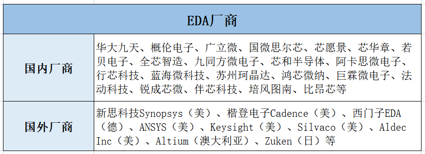
It is well known that the global EDA market is oligopolistic and highly concentrated. Synopsys, Cadence, Siemens EDA (formerly Mentor Graphics, acquired by Siemens in 2016 and officially renamed Siemens EDA in 2021), and ANSYS are referred to as the “Big Four” in EDA software. Public information shows that they account for nearly 80% of the global EDA market. The monopoly of the “Big Four” may stem from their ability to provide a complete set of EDA tools covering the entire product chain from front-end design, back-end design, simulation/verification to tape-out, forming a closed loop in design; or from their careful management in their areas of expertise, forming unique advantages in different stages of chip design and manufacturing processes, playing a key role. In addition, foreign EDA manufacturers such as Keysight, Silvaco, Aldec, Altium, and Zuken continue to deepen their expertise in their respective fields.
Although domestic EDA manufacturers started relatively late, the continuous deepening of the domestic chip industry chain has led to a sharp increase in public attention to upstream EDA. With the diversified development of domestic chip upstream and downstream fields, especially in recent years, the acceleration of industrialization of emerging technologies such as 5G, artificial intelligence, and autonomous driving, as well as the transformation and upgrading of traditional manufacturing industries, has led to a surge in chip demand, and the Chinese semiconductor market is booming, resulting in a rapid increase in demand for domestic EDA [5]. In the context of almost foreign monopoly, a batch of independent EDA manufacturers has emerged in China, represented by Huada Jiutian, Gai Lun Electronics, Guangli Micro, Guowei Si Erxin, Xin Yuanjing, Xin Huazhang, Ruobe Electronics, Quanxin Intelligent Manufacturing, Jiutongfang Microelectronics, and Xin He Semiconductor, capturing a certain market share. As a result, many excellent EDA unit software have emerged, and each manufacturer is developing towards local solutions and full-process solutions based on their advantages in segmented fields.
Table 3 EDA Manufacturers
◉ Chip Manufacturing Equipment
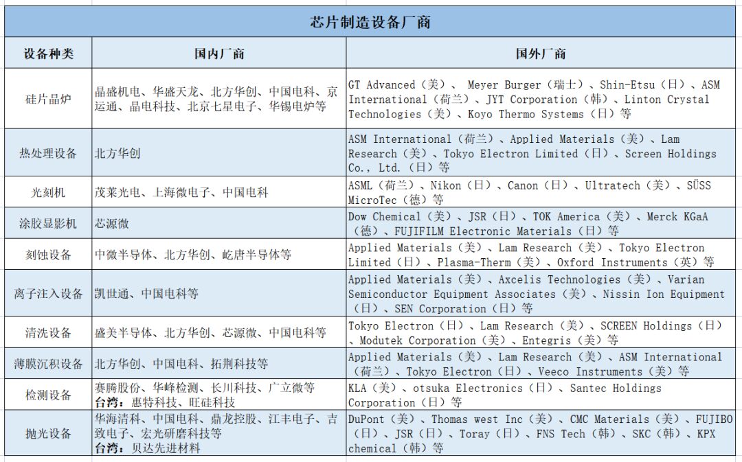
Chip equipment typically has three characteristics. First, the R&D time is long; the development of a new device takes at least five years and up to ten years, and it needs continuous improvement and optimization during use. Second, the investment amount is large; for example, Dutch photolithography giant ASML has invested over 2 billion euros annually for 20 consecutive years to develop EUV equipment. Third, it is highly monopolistic; the five major giants from the US, Japan, and Europe lead the global semiconductor equipment market, namely Applied Materials, ASML, Lam Research, Tokyo Electron, and KLA. For instance, ASML in the Netherlands holds over 90% market share in the photolithography market, especially in the extreme ultraviolet lithography (EUV) field, where it has an absolute monopoly; American Applied Materials is a leader in the ion etching and thin film deposition sectors, holding a place in etching, cleaning, and ion implantation equipment; and American Lam Research is a global leader in etching equipment.
In recent years, supported by national policies, domestic chip equipment manufacturers have gradually developed. In various segments of chip equipment, breakthroughs have been made from 0 to 1 in polishing equipment, cleaning equipment, etching equipment, and physical vapor deposition (PVD) equipment. Zhongwei Semiconductor’s 12-inch etching machine has successfully been used in TSMC’s 5nm production; Shengmei Semiconductor’s cleaning equipment has entered multiple domestic production lines; and China Electronics Technology’s ion implantation equipment has successfully achieved the localization of all series of ion implantation machines; Huahai Qingke’s chemical-mechanical polishing (CMP) equipment has achieved full coverage of all processes for 28nm processes; and ChipSource Micro’s photolithography coating and developing equipment and single-wafer wet processing equipment have been applied as mainstream models in leading domestic manufacturers such as TSMC, Changdian Technology, Huada Technology, and Tongfu Microelectronics. The main manufacturers in various segments of chip equipment are shown in Table 4.
Table 4 Chip Manufacturing Equipment Manufacturers
◉ Chip Manufacturing Materials
From the perspective of the chip production process, materials and equipment are the physical foundation of chip manufacturing, and the scale of raw material production directly relates to the development of the chip industry. Currently, the chip materials in China are a relatively weak link in the industry chain, mainly due to the late start of the industry, being at a disadvantage in terms of variety richness and competitiveness. For example, the global silicon wafer market is mainly dominated by a few manufacturers such as Shin-Etsu and SUMCO, while China’s silicon wafer industry started late and currently focuses mainly on supplying 8-inch and below silicon wafers, which cannot meet mainstream demand; the photomask market is mainly led by US and Japanese leading enterprises, with high industry concentration, where the top three photomask manufacturers are Photronics from the US, Dai Nippon Printing from Japan, and Toppan from Japan.
With the continuous large-scale construction of the domestic chip market, domestic chip materials have ushered in rapid development. At the same time, relying on industrial policy guidance and product price advantages, local enterprises have achieved breakthrough progress in their respective fields. For example, Shanghai Silicon Industry has mastered the entire core technology of silicon wafer production, including 300mm silicon wafers; Huate Gas’s germane, high-purity ethylene, and high-purity propylene have achieved application breakthroughs in electronic special gases, especially in the field of high-end chip materials; Jiangfeng Electronics’ target products have been applied in the most advanced manufacturing processes of world-renowned semiconductor manufacturers represented by TSMC; and Anji Technology has successfully broken the monopoly of foreign manufacturers on chemical mechanical polishing liquids, some functional wet electronic chemicals, electroplating liquids, and additives in the integrated circuit field, achieving technological breakthroughs in three core products in specific fields. The main manufacturers in various segments of chip materials are shown in Table 5.
Table 5 Chip Manufacturing Material Manufacturers
2. Midstream Analysis of the Chip Industry Chain
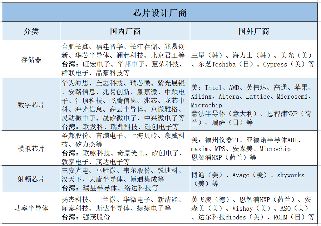
The chip design industry has extremely high technical barriers, requiring significant human and material investment, and a long accumulation of technology and experience. China’s shortcomings in chip design are very obvious, with significant gaps between high-end general-purpose chips and advanced foreign levels, mainly in central processing units (CPUs), memory, and high-end general-purpose chips (including FPGA, AD/DA, etc.). Currently, the CPU field is almost monopolized by Intel in the global market. The memory field is primarily dominated by foreign manufacturers such as Samsung, Hynix, and Micron. The US has a clear advantage in digital chip design, with many world-class design companies such as Intel, Qualcomm, NVIDIA, and AMD. Additionally, international manufacturers like Infineon, NXP, and Toshiba also hold a place in various segments of chip design.
In recent years, China’s chip design industry has maintained a trend of rapid growth driven by factors such as improving self-sufficiency, policy support, specification upgrades, and innovative applications. From the current state of the industry, there are many excellent chip design manufacturers emerging in areas such as radio frequency chips, memory chips, graphics processing units (GPUs), and communication chips. For example, in the memory field, Yangtze Memory Technologies has achieved mass production of 64-layer 3D NAND flash memory and is developing 128-layer products; GigaDevice ranks among the top in the Nor Flash market; in the radio frequency chip field, Zhaoxin Micro has completed a comprehensive layout of all categories of RF front-end through continuous innovation and independent R&D. Huawei HiSilicon and Unisoc have become important chip design manufacturers in the mobile communication field and have entered the top ten Fabless suppliers globally in terms of output value; ZTE Microelectronics’ RoseFinch7100 is China’s first independently developed NB-IoT secure IoT chip; and Jingjia Micro is a major player in the domestic GPU market and the only company in China to independently develop GPUs for commercial use. The main manufacturers in chip design are shown in Table 6.
Table 6 Chip Design Manufacturers
 Chip manufacturing is the most core and challenging link in the chip industry chain, involving complex process flows, precision equipment, high investments, and strict quality control. Asia holds a leading position in chip manufacturing, especially Taiwan and South Korea, where Taiwan’s TSMC and South Korea’s Samsung are the largest chip manufacturers globally, possessing leading process technologies. In addition, the main foundries among global chip manufacturers include UMC, Global Foundries, TowerJazz, PowerChip, Vanguard International Semiconductor, Dongbu HiTek, X-Fab, SSMC, etc. Currently, the more advanced chip manufacturers in mainland China include SMIC, which has begun mass production of its latest 14nm process. In addition, there are several chip manufacturing companies such as Hua Hong Semiconductor, Sanan Optoelectronics, Silan Microelectronics, Huahai Microelectronics, Changxin Storage, and Yangtze Memory Technologies, which are quietly developing.
Although China’s chip manufacturing has reached the level of 14nm and below, there is still a significant gap compared to the international leading level. For example, in the 7nm and below process, the production capacity and quality of China’s chip manufacturers have yet to meet market demand. At the same time, due to the high-quality chip manufacturing equipment being monopolized by foreign countries, China’s development in chip manufacturing is relatively lagging. For instance, photolithography machines are key equipment required for chip manufacturing, but the high-end photolithography machine market has been monopolized by foreign countries.
Chip manufacturing is the most core and challenging link in the chip industry chain, involving complex process flows, precision equipment, high investments, and strict quality control. Asia holds a leading position in chip manufacturing, especially Taiwan and South Korea, where Taiwan’s TSMC and South Korea’s Samsung are the largest chip manufacturers globally, possessing leading process technologies. In addition, the main foundries among global chip manufacturers include UMC, Global Foundries, TowerJazz, PowerChip, Vanguard International Semiconductor, Dongbu HiTek, X-Fab, SSMC, etc. Currently, the more advanced chip manufacturers in mainland China include SMIC, which has begun mass production of its latest 14nm process. In addition, there are several chip manufacturing companies such as Hua Hong Semiconductor, Sanan Optoelectronics, Silan Microelectronics, Huahai Microelectronics, Changxin Storage, and Yangtze Memory Technologies, which are quietly developing.
Although China’s chip manufacturing has reached the level of 14nm and below, there is still a significant gap compared to the international leading level. For example, in the 7nm and below process, the production capacity and quality of China’s chip manufacturers have yet to meet market demand. At the same time, due to the high-quality chip manufacturing equipment being monopolized by foreign countries, China’s development in chip manufacturing is relatively lagging. For instance, photolithography machines are key equipment required for chip manufacturing, but the high-end photolithography machine market has been monopolized by foreign countries.
Moreover, the CIM (Computer Integrated Manufacture) system, which is extremely important for the chip manufacturing process, is also monopolized by American tech giant IBM and American semiconductor equipment giant Applied Materials. The CIM system consists of dozens of software systems, including Manufacturing Execution Systems (MES), Equipment Control Platforms (EAP), Yield Management Systems (YMS), FAB Real-Time Scheduling Systems (RTS), etc., also known as “EDA for the manufacturing process.” The products in the market mainly come from IBM and Applied Materials, which continuously enhance their strength through first-mover advantages, occupying the main market for 12-inch wafers and above. In this field, there are very few domestic participants, with major manufacturers including Ge Rui Li, Shang Yang Software, Sai Mei Te, Xin Xiang Technology, Shanghai Kai Bo, Ge Chuang Dong Zhi, and Huajing Information, gradually achieving breakthroughs in CIM projects for 6-inch, 8-inch, and 12-inch wafer fabs.
Table 7 Chip Manufacturing Manufacturers
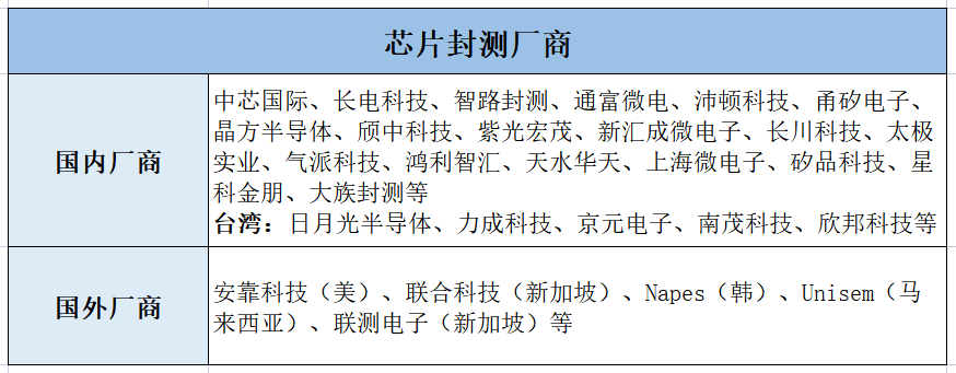
It is worth mentioning that China has strong capabilities in the packaging testing field, with a number of competitive and scalable enterprises. According to data from the Chip Thought Research Institute, the estimated ranking of the top ten global packaging testing companies in 2022 is: ASE, Amkor Technology, JCET, Tongfu Microelectronics, Powertech Technology, Tianshui Huatian Technology, Zhilu Packaging, King Yuan Electronics, Chipbond Technology, and Nanmao Technology. It can be seen that among the top ten, only the second-ranked Amkor Technology is a US company, accounting for about 14%, while the other nine manufacturers are all Chinese companies, collectively holding a market share of 64%, accounting for nearly two-thirds of the global packaging testing market.
Domestic packaging testing companies not only provide quality services for domestic and foreign customers but also support domestic independent innovation and have accumulated advanced packaging technology. Among them, advanced packaging technologies such as Ball Grid Array (BGA), Wafer Level Chip Scale Packaging (WLCSP), and Single Inline Package (SIP) have already achieved mass production.
Table 8 Chip Packaging Testing Manufacturers
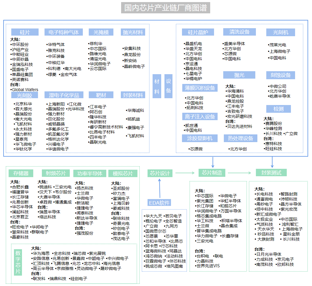
Figure 3 Domestic Chip Industry Chain Manufacturer Map
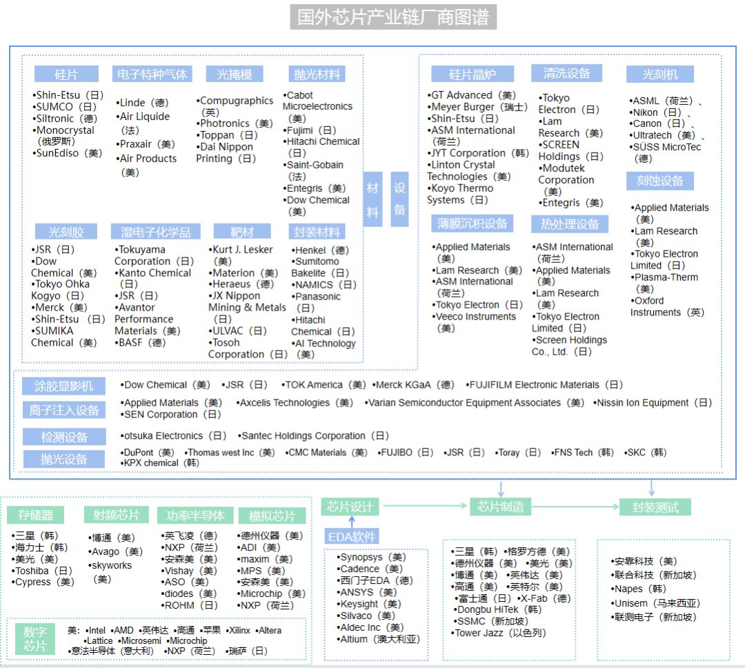
Figure 4 International Chip Industry Chain Manufacturer Map
The chip industry requires huge investments and is highly competitive, involving many complex technologies, process flows, materials, and manufacturing equipment. The global chip industry chain is a continuously innovative ecosystem, and companies in the chip industry chain need to establish differentiated positions and find their unique value and competitive advantages within the industry chain. The widespread application of artificial intelligence technology has created a huge demand for computing power, becoming one of the core driving forces for chip industry development. Time is the most objective witness; decades of development have witnessed the vigorous growth of the chip industry. On this endless track, chip manufacturers must break through technological bottlenecks and strengthen industry chain collaboration to navigate through challenges and achieve sustainable development.
References
[1] 2022 In-depth Analysis of China’s Semiconductor Industry Chain, Competition Pattern Analysis of Sub-fields
[2] The Long Way Ahead: Comprehensive Review of the Chip Industry Chain
[3] Popular Science on Chinese Chip Enterprises | List of Leading Enterprises in Various Sub-fields of China’s Chips
[4] Detailed Analysis of the Full Chip Industry Chain
[5] “Analysis Report on IC Design and Tool Chain in Mainland China”