The artificial tactile system is a core component of human-machine interfaces (HMI), widely used in fields such as robotic prosthetics and bioelectronic skin. With the development of the Internet of Things (IoT), the demand for real-time intelligent interaction is increasing, and the next generation of tactile systems is expected to simulate human tactile recognition capabilities while possessing energy-efficient computing capabilities. Although traditional research has focused on enhancing sensor performance, large-scale tactile networks still face critical challenges such as excessive power consumption, transmission delays, and computational bottlenecks. Therefore, research trends are gradually shifting towards monolithic system-level architectures, embedding computational functions within sensor units to improve energy and processing efficiency.
Monolithic 3D (M3D) integration is proposed as a potential solution for the next generation of artificial tactile systems, achieving low power consumption and fast response through short vertical interconnections between components. Meanwhile, significant advancements have been made in piezoelectric materials such as lead zirconate titanate (PZT) and polyvinylidene fluoride (PVDF) copolymer (P(VDF-TrFE)). These materials respond quickly and can self-power, operating at low power without the need for an external power source when integrated with CMOS circuits, making them highly attractive for artificial tactile sensing applications. However, the limited compatibility of piezoelectric materials with traditional silicon-based manufacturing processes poses challenges for achieving monolithic integrated artificial tactile sensing systems. Additionally, traditional piezoelectric sensors typically respond only to dynamic signals, fundamentally limiting their application range.
According to MEMS Consulting, to address these issues, a research team from the Korea Advanced Institute of Science and Technology (KAIST) and Hanyang University proposed a monolithic 3D integrated tactile sensing system that combines piezoelectric sensors with ferroelectric field-effect transistors (FeFETs), enabling direct processing of static and dynamic pressure signals at the sensor nodes. This system utilizes multi-level storage states to achieve analog noise filtering within the sensor, featuring high sensitivity and ultra-low power characteristics, providing a promising platform for the next generation of tactile human-machine interfaces. The related research results were published in the journal Advanced Functional Materials under the title “Near-Sensor Analog Computing via Monolithic 3D Piezoelectric Sensor–FeFET for Tactile Sensing System.”
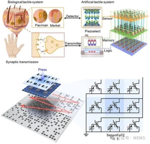
Figure 1: Graphic abstract of this study
This research work demonstrates a monolithic 3D integrated near-sensor analog computing system that combines CMOS-compatible aluminum nitride (AlN) piezoelectric sensors with metal-ferroelectric-metal-insulator-semiconductor (MFMIS) structure FeFETs, enabling direct processing of dynamic and static tactile signals at the sensor nodes without external interface circuits. The proposed sensing-computing unit (composed of the piezoelectric sensor and MFMIS FeFET) can detect static pressure signals, with a signal hold time exceeding 100 s, and can clearly distinguish pressure levels with a sensitivity of 18.3 Pa⁻¹. Furthermore, by adjusting the capacitance ratio of CDE to CFE in the MFMIS FeFET as the local processing unit, three different output levels can be generated under the same mechanical stimulus, laying the foundation for analog multiply-accumulate (MAC) operations.
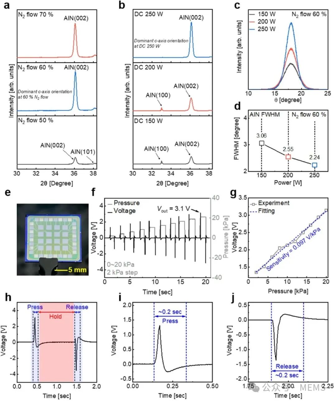
Figure 2: Structure and electrical characteristics of AlN piezoelectric sensors
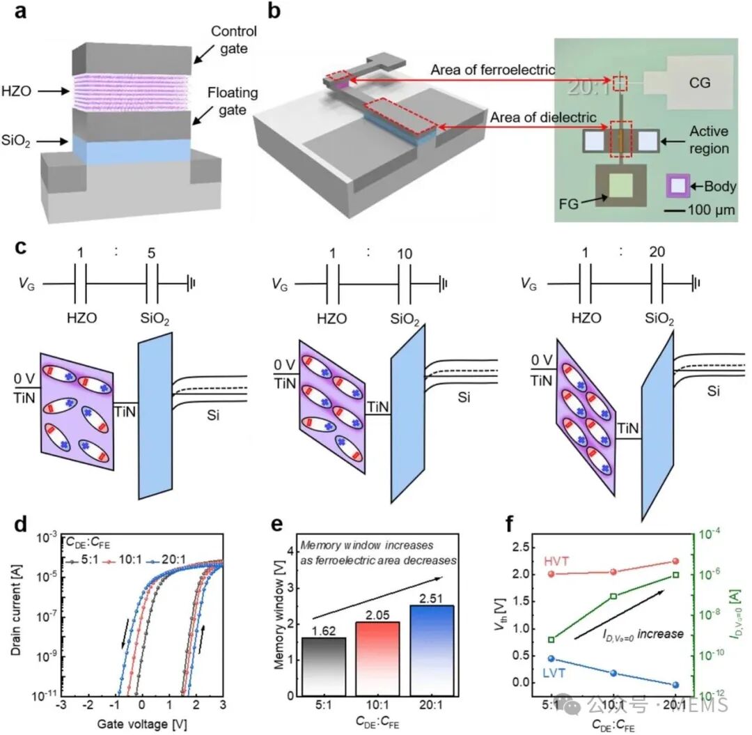
Figure 3: Structure and electrical characteristics of MFMIS devices
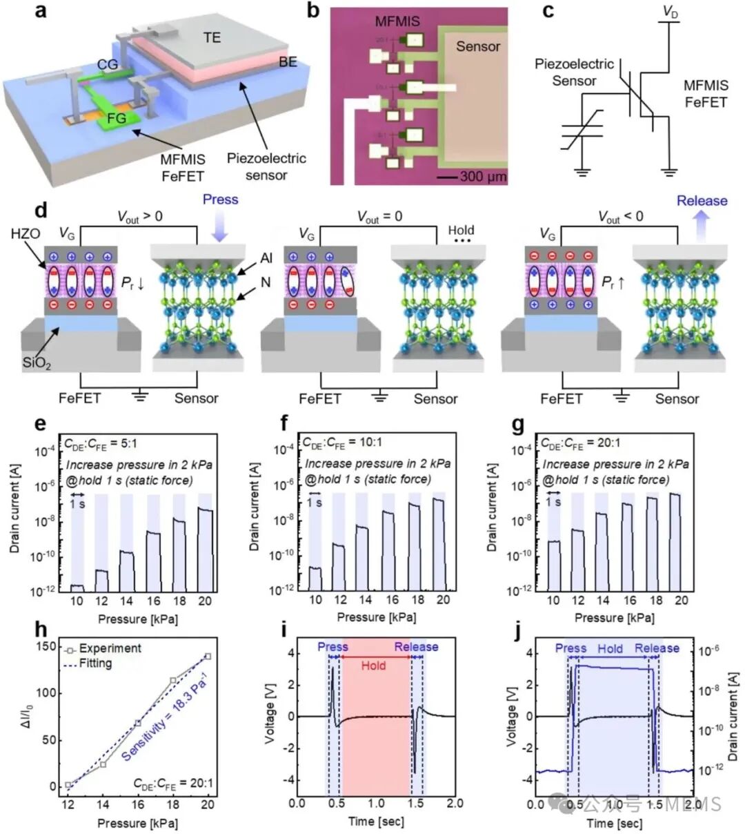
Figure 4: Static detection based on integrated piezoelectric sensors and MFMIS FeFET units
To develop the proposed sensing-computing unit into the next generation of artificial tactile systems, the researchers expanded it into an array structure based on a 3 × 3 kernel and validated its ability to simultaneously capture tactile inputs and suppress noise through Braille-inspired patterns. By assigning Gaussian-distributed kernel weights to each unit, the array can achieve analog spatial filtering, eliminating noise while maintaining the fidelity of tactile patterns— a performance that is difficult to achieve with traditional uniform averaging kernels. Additionally, the maximum power consumption of this system is only about 10 nW, which is approximately 500 times lower than that of resistive-memristor systems (typically several microwatts), and over five orders of magnitude higher in energy efficiency compared to traditional amplifier ADC-MAC architectures. These results define a new class of integrated tactile processors capable of achieving real-time, energy-efficient computing at the sensor nodes.
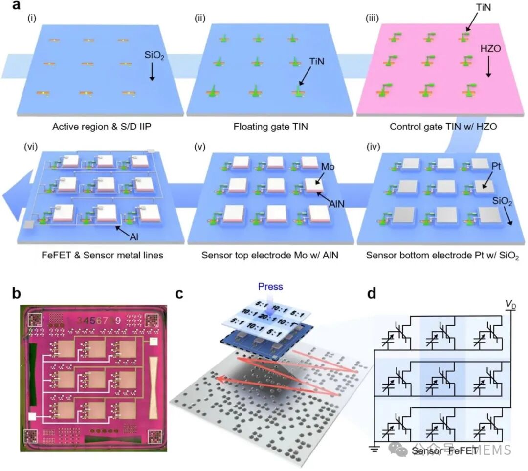
Figure 5: Schematic diagram of the monolithic 3D tactile sensing system
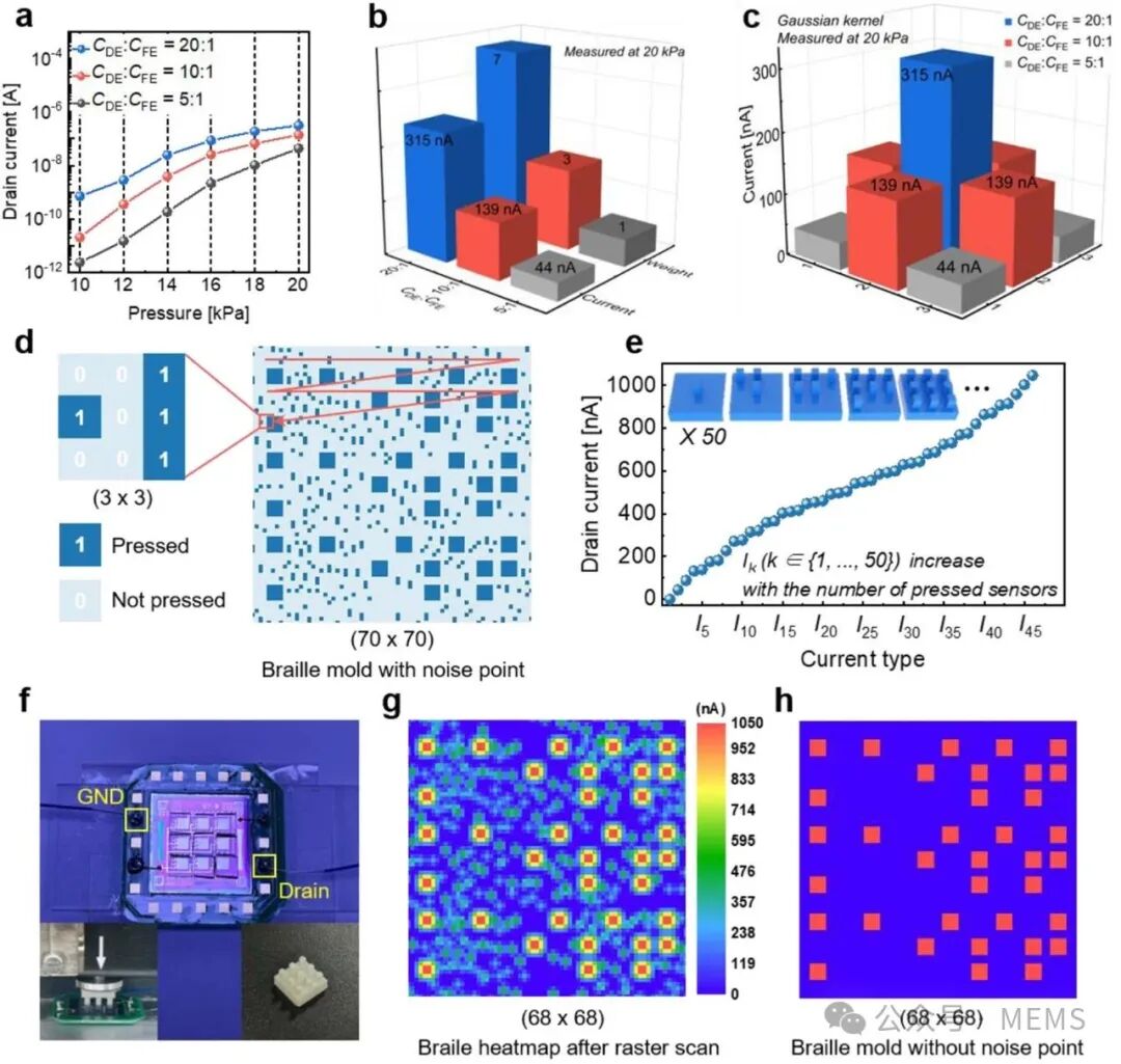
Figure 6: Pressure stimulation noise suppression using a monolithic 3D tactile sensing array
This research demonstrates the application potential of a near-sensor analog computing system based on piezoelectric sensors and ferroelectric field-effect transistors in next-generation high-energy-efficiency tactile sensing platforms. This monolithic integration of sensing and computing provides a scalable and CMOS-compatible foundation for future electronic skin, robotic perception, and neuromorphic interfaces with embedded intelligence. Furthermore, the analog current output generated by this system can be easily converted into pulse signals, facilitating future integration with neuromorphic processors, thereby promoting the development of low-latency, biomimetic human-machine interface systems.
Paper Information:
https://doi.org/10.1002/adfm.202516545