 This is the 219th content shared by the platform.
Part 1
1. Demand Analysis and Chip Selection
1.1 Function Requirement Definition
Clearly define project goals, such as whether it needs to support 3-channel 12-bit ADC sampling , UART/SPI/I²C communication , or low power mode (5μA standby power) and other features.
 Though small, it is fully equipped.
- Arm Cortex-M0+ core, 16KB flash + low-power timer, balancing performance and energy efficiency;
- 3-channel 12-bit ADC + 6 GPIOs, precise control without compromise;
- Supports UART/SPI/I2C, easily compatible with mainstream communication protocols;
- -40°C~125°C wide temperature operation, stable in extreme environments!
1.2 Performance Indicator Setting
Determine the adaptability of parameters such as 24MHz main frequency , 1KB SRAM capacity , and -40°C~125°C temperature range based on application scenarios (e.g., medical wearable devices, consumer electronics).
Application Scenarios Addressing Pain Points
- Medical wearables: blood glucose probes, portable monitors;
- Consumer electronics: TWS earbuds, smart rings;
- Industrial sensing: micro sensors, edge nodes.
MSPM0C1104 vs. Mainstream MCU Performance Comparison Table
|
Parameter |
MSPM0C1104 |
Competitor A (STM32L0 series) |
Competitor B (NXP LPC800 series) |
|---|---|---|---|
|
Core |
Arm Cortex-M0+ |
Cortex-M0+ |
Cortex-M0+ |
|
Main Frequency |
32MHz |
32MHz |
30MHz |
|
Flash/Memory |
16KB/2KB |
16KB/4KB |
16KB/4KB |
|
ADC Channels/Resolution |
3 channels/12 bits |
1 channel/12 bits |
2 channels/12 bits |
|
Communication Interface |
UART/SPI/I2C |
UART/SPI/I2C |
UART/SPI/I2C |
|
Number of GPIOs |
6 |
8 |
10 |
|
Package Size |
1.38mm² |
2.2mm² |
2.5mm² |
|
Operating Temperature |
-40°C ~ 125°C |
-40°C ~ 85°C |
-40°C ~ 105°C |
|
Unit Price (thousand pieces in bulk) |
$0.16–0.20 |
$0.25–0.30 |
$0.22–0.28 |
Part 2
2. Hardware Development
2.1 Schematic Design
Design peripheral interface circuits based on chip pin assignments (e.g., 6 GPIOs) integrating buzzer drivers or sensor modules, optimizing power management circuits to accommodate 1.62V–3.6V wide voltage input requirements.
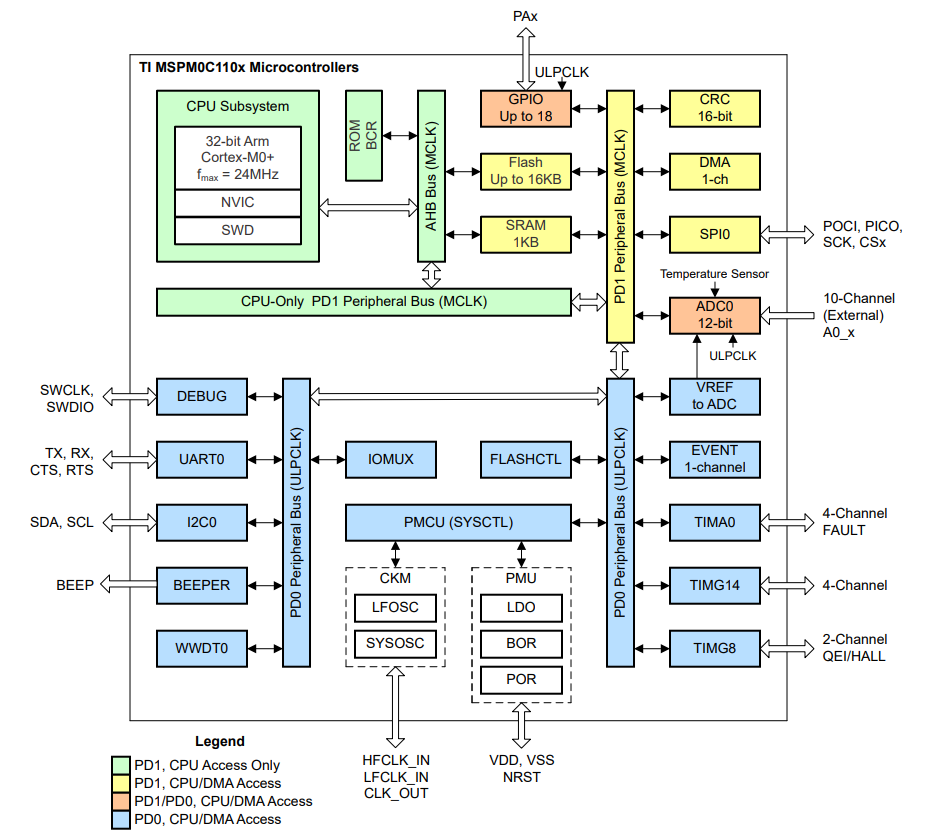
Figure: Functional Block Diagram of MCU MSPM0C110x (Source: TI Official Website)
2.2 PCB Layout and Manufacturing
Adopt a compact layout to match the micro-packaging requirements of the 1.38mm² wafer package (TI: DSBGA package, commonly referred to as CSP package), following signal integrity rules to reduce high-frequency signal interference.
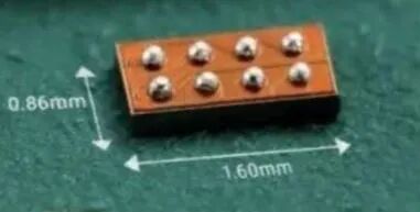
Figure: MCU MSPM0C1104 DSBGA Package (Source: From the Internet
The development tools and related support for MSPM0C1104 are as follows:
- LP-MSPM0C1104 LaunchPad™ Development Kit
Includes evaluation modules and onboard TIXDS110 debugging probe, supporting programming and debugging functions, enabling rapid system development.
- Zero Code Studio Toolchain
Provides a graphical configuration interface, supporting rapid initialization code generation and parameter configuration, lowering the development threshold.
- Pin Compatibility Extension
Compatible with other package models of the MSPM0 series, facilitating a smooth transition from prototype validation to mass production design.
- Low-Cost Support
The development kit and toolchain are designed for low-cost needs, suitable for miniaturized application scenarios such as medical wearables and consumer electronics.
Cost-Performance King
- $0.16–0.20 (bulk price), low cost driving high performance;
- TI MSPM0 series smallest member, seamlessly compatible with the Arm ecosystem, low development threshold!
Part 3
3. Software Development
3.1 Development Environment Setup
- Use the LP-MSPM0C1104 LaunchPad development kit and accompanying IDE (such as TI official toolchain), providing hardware prototype validation and debugging interfaces;
- Configure DMA controller and ADC sampling parameters to enhance data processing efficiency.
3.2 Code Generation and Optimization
- Utilize the Zero Code Studio graphical tool to quickly generate initialization code, simplifying register configuration and code generation;
- Optimize using the Arm Cortex-M0+ instruction set to reduce power consumption (operating mode 87μA/MHz).
Part 4
4. Debugging and Testing
4.1 Hardware Debugging
- Module verification of ADC accuracy, communication protocol stability, and 5V fault-tolerant I/O performance;
- Use the TIXDS110 debugging probe to monitor real-time operating status, supporting real-time tracking and power consumption analysis.
4.2 Software Testing
- Execute unit tests (such as SRAM data read/write verification) and integration tests;
- Verify SRAM data retention functionality in low power mode.
Part 5
5. Mass Production and Maintenance
5.1 Small Batch Trial Production
Test wide temperature adaptability (-40°C~125°C) and long-term operational stability.
5.2 Mass Production
Quickly switch to other models in the same series (such as higher storage capacity versions) based on pin compatibility design.
5.3 Software Iteration
Optimize driver code or add communication protocol support based on user feedback.
——The End——
 Today’s sharing ends here. If you want to know more, you can contact [email protected] or call 010-62901860-639/609/611 for details.
If you are interested in more popular chip information on the market, you can click “Read the original text” to visit the IPBrain website for inquiries.

「Previous Recommendations」
Texas Instruments BQ76200, low power, high-side N-channel system chip—”customized” for high-power lithium-ion batteriesAfter the US has imposed a cumulative 104% tariff, prices may rise at any timeAD9695, a 14-bit 1300/625MSPS high-speed ADC chip from Analog Devices, priced at 20,000Texas Instruments TPS3125 power monitoring chip: the guardian of electronic systems