Optimization Guide for Hardware Compatibility Design of NXP S32K324 and S32K328
Keywords:Power Management, Wake-up Timing, SBC Compatibility, PG Signal

Background Information
A certain project platform uses theS32K324+FS2613 solution, and its wake-up process is as follows:
1.Wake-up Sources:ACC/IGN, CAN_INH, IMU_INT and other signals trigger the MCU wake-up, using the MCU wake-up solution.
2.Wake-up Process:In sleep mode, the S32K324 only requires 3.3V power supply (internal LDO converts to 1.1V for core power), and after receiving the wake-up signal, it wakes up and enters low-speed mode, notifying the FS2613 to wake up through theCS pin.
3.Power Switching:After the FS2613 is awakened, it outputs 1.5V power, and the MCU switches to normal mode (to avoid excessive power consumption from directly using the internal LDO).
After upgrading toS32K328, due to power consumption differences (the 328 requires external 1.5V power during the wake-up phase and cannot switch internally to 1.1V), the original solution encounteredissues where it could not wake up under specific conditions. The following is an analysis of the optimization plan.
Compatibility Plan Comparison
Plan 1: FS2613+S32K328 (without EXTWAKE/PG signal connection)
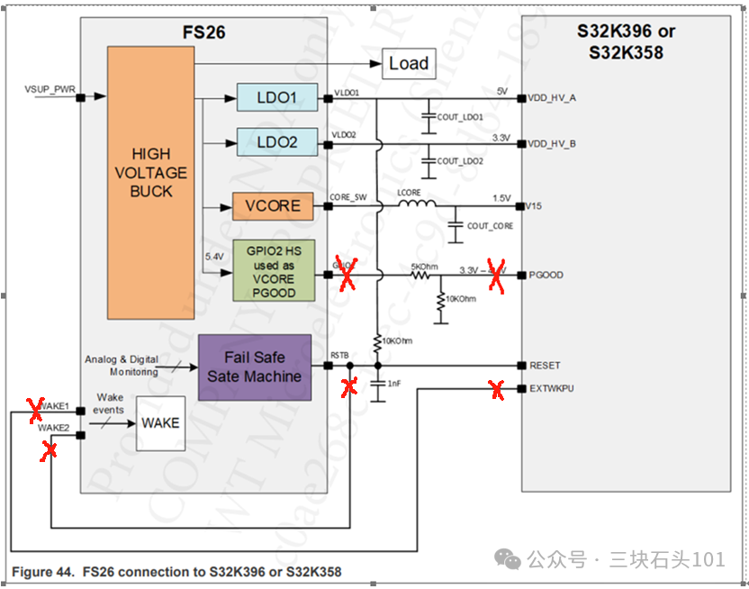
Problem Description:
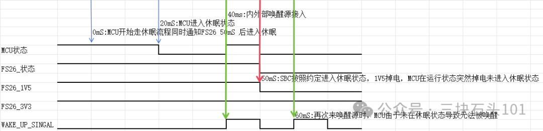
·When the MCU is in sleep mode and the SBC is not in sleep mode, an external wake-up triggers the MCU to wake up, but the SBC turns off 1.5V according to the protocol, causing the MCU to power off abnormally and unable to recover. Root Cause Analysis:
·The S32K328 relies on external 1.5V power, while the FS2613 does not provide a PG (Power Good) signal feedback for power status, leading to a wake-up timing conflict.
The timing in this wake-up scenario is approximately as follows:
Plan 2: FS2613+S32K328 (with EXTWAKE/Reset function enabled)
Improvements:
·By using theEXTWAKE pin to transmit the wake-up signal to the SBC, the MCU delays 50ms after outputting the EXTWAKE wake-up signal (waiting for FS26 to wake up and stabilize 1.5V) before switching to run mode. Remaining Issues:
·If the SBC unexpectedly turns off 1.5V, the MCU will trigger a Reset and power back on, leading tounexpected power loss, which may cause data anomalies.
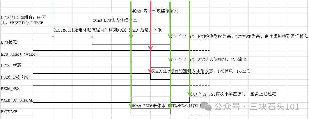
Timing Conflict Example: 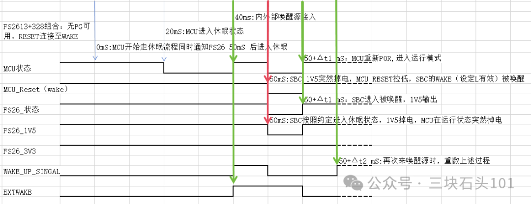
Plan 3: FS2633+S32K328 (with EXTWAKE+PG signal enabled)
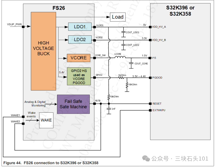
Ultimate Solution:
·Replace the SBC withFS2633, utilizing its GPIO2 pin to provide 1.5V PG signal.
·Cooperation Logic:
1.When the SBC is in sleep mode, PG is pulled low, and the EXTWAKE wake-up signal is suspended.
2.After the wake-up signal is triggered, the SBC outputs 1.5V and pulls PG high.
3.After the MCU detects PG as high and EXTWAKE as low, it enters run mode. Advantages:
·Completely resolves the abnormal power loss issue, ensuring power stability before switching modes. Potential Drawbacks:
·There is a slight delay in wake-up response (see timing diagram).
Key Design Review
1.Prioritize Plan 3:Pairing FS2633 with PG signal to ensure reliable wake-up timing.
2.PG Signal Monitoring:GPIO2 of FS2633 must be strictly used for 1.5V status feedback, in conjunction with EXTWAKE to achieve a reliable wake-up solution.
3.Testing for Abnormal Scenarios:Focus on verifying boundary conditions for SBC power switching during MCU sleep.