(Source: Semiconductor Industry Observation)
In recent years, with the acceleration of global energy transition, the fields of photovoltaic power generation and variable frequency control have experienced explosive growth. As the core control devices in this field, the performance of MCU chips directly determines the efficiency, reliability, and cost competitiveness of the systems. Huatai Electronics’ MCU, developed based on the ARM dual-core Cortex-M7 architecture, has been widely used in photovoltaic inverters and industrial variable frequency drives. However, facing the ecological barriers of international giants and the high migration costs of customer systems, how to break through the market trust bottleneck has become a key issue. Recently, Huatai Electronics’ SOC product line has successfully built an inverter system for full-scene verification of its chips, proving its technological maturity and opening up new paths for market competition.
1 Industry Pain Point: High Migration Costs of Customer Systems
In the field of industrial control, the selection of MCU chips is often deeply tied to the system architecture. A certain photovoltaic inverter manufacturer once reported: “The existing solution has used imported MCUs for three generations, with over a million lines of code invested in underlying drivers, power management, communication protocols, etc. Replacing the main control chip is equivalent to reconstructing the entire system.” This technical lock-in effect is particularly pronounced in the industrial sector, manifested in three aspects: Hardware compatibility challenges: Peripheral circuit design and power device drive parameters need to be precisely matched with MCU characteristics. Software ecosystem dependency: RTOS, algorithm libraries, development toolchains, etc., have formed a complete technical stack. Certification system barriers: Photovoltaic inverters must pass dozens of industry certifications such as grid connection certification and EMC testing. These practical issues lead customers to be hesitant to use domestic chips, even if performance parameters are similar, the replacement decision still faces significant technical risks.
Huatai Electronics’ MCU adopts a software and hardware ecosystem construction, including SDK, graphical configuration design, integrated development environment CPS, and also employs diversified system DEMO designs, sharing design solutions with customers, providing on-site support services, and online support that can dynamically respond 24/7 to maximize assistance for customer system migration.
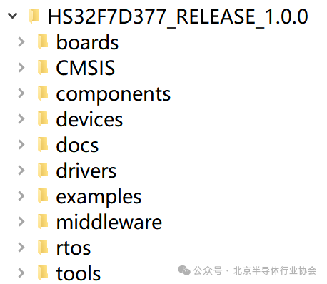
Figure 1. SDK Structure Diagram
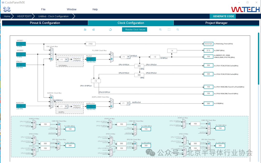
Figure 2. Graphical Configuration Environment CPMX Interface
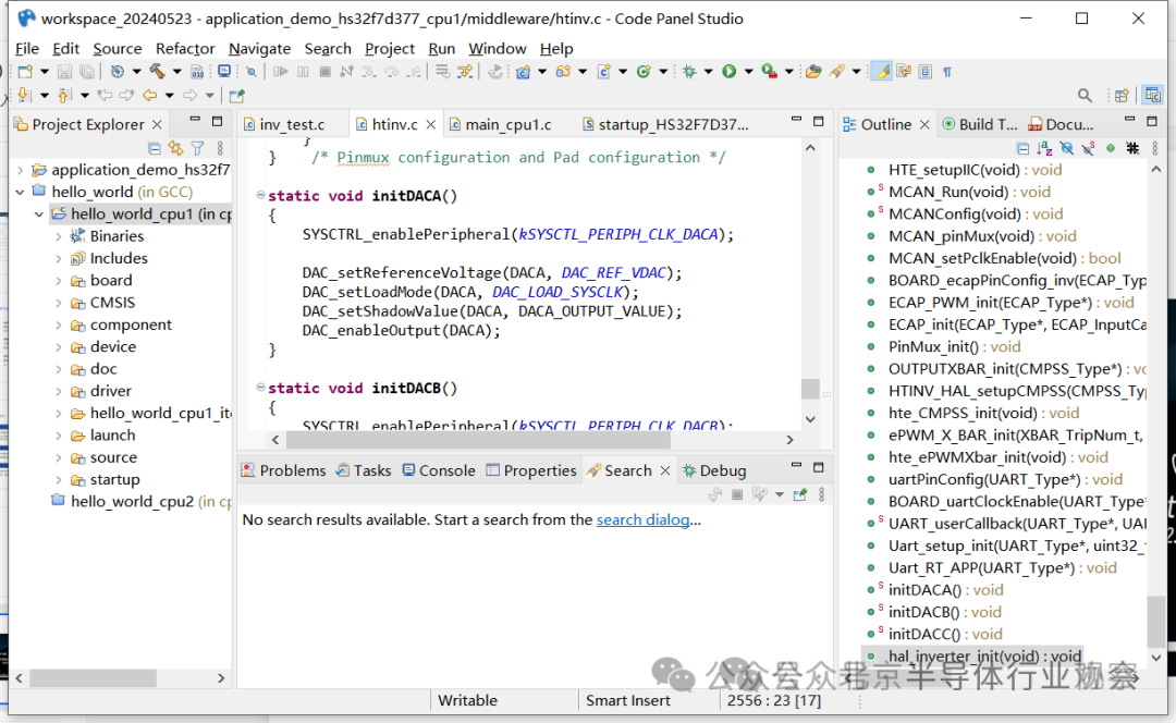
Figure 3. Integrated Development Environment CPS Interface
2 Technological Breakthrough: Differentiated Advantages of Dual-Core M7 Architecture
Huatai’s developed MCU chip adopts a dual-core Cortex-M7 design, with a main frequency of 300MHz, equipped with 2MB eFlash and 512kB SRAM, directly addressing the core needs of industrial control in its architecture design: Parallel computing capability: The dual-core architecture allows for physical isolation of control algorithms and communication protocols, such as parallel processing of photovoltaic MPPT algorithms (Core 1) and CAN/Modbus communication (Core 2), reducing response latency by 40%. High-precision PWM control: 16-bit PWM resolution combined with hardware dead-time control improves control accuracy in inverter applications, thereby enhancing product efficiency. Functional safety design: The dual-core design scheme meets the redundancy design requirements for software control in photovoltaic systems. Compared to single-core solutions, this chip has also shown significant advantages in testing: under full load conditions, THD (Total Harmonic Distortion) remains stable within 2%, and MPPT tracking efficiency reaches 99.6%, with performance indicators reaching international first-tier levels.
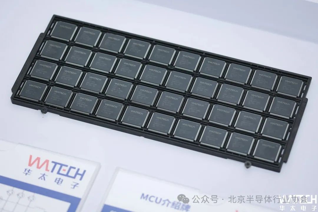
Figure 4. Huatai ARM Dual-Core Cortex-M7 MCU
3 Verification System: Forward Development from Chip to System
To break the customer’s skepticism about “paper parameters”, Huatai Electronics innovatively constructed a three-level verification system of “chip-module-system”: Benchmark testing platform built on JTAG boundary scan automated testing system, conducting 30*24 hours of stress testing on key indicators such as ADC sampling accuracy (±0.3%), PWM timing jitter (<5ns), establishing a complete parameter confidence interval. Reference design development targeting photovoltaic inverter scenarios, launching a turnkey solution that includes LLC resonant control, three-level topology drive, and RS485 isolated communication. By encapsulating the underlying drivers with a hardware abstraction layer (HAL), the customer code migration workload is reduced by 70%. In the reference design, Huatai Electronics adopted a unique ultra-low loss SJ IGBT core device, making the overall solution more efficient and energy-saving. System-level empirical evidence from a self-built photovoltaic experimental power station shows that the 6kW household energy storage inverter equipped with this chip has been running continuously for 180 days, with data showing: daily power generation increased by 2.3% compared to benchmark products, and the failure rate is less than 0.5 times per thousand hours. Especially under extreme conditions such as -25°C low-temperature startup and a sudden 10% increase in grid voltage, the system has passed tests stably. The 6kW household energy storage inverter system is an efficient energy storage solution suitable for home environments. This system can convert the direct current generated by solar panels into alternating current and store excess electricity for use at night or on cloudy days. Key features include: DC-AC inverter system: This system is the key part that converts direct current (DC) into alternating current (AC). This conversion is crucial in household storage system applications, allowing PV or DC stored in batteries to be used by household appliances, the grid, or other devices requiring AC. The DC-AC inverter system is responsible not only for the conversion of electrical energy but also for controlling output voltage and frequency, ensuring the quality and stability of the output electrical energy. DC-DC battery charging and discharging system: This system’s main task is to convert the direct current from the bus into an output voltage suitable for battery charging and discharging, which can be adjusted through methods such as LLC. At the same time, it adjusts the output voltage and current according to the battery’s status and needs, and monitors the battery’s status through BMS to ensure the charging and discharging process occurs within a safe range. PV boost system: This system uses a certain number of solar panels to raise the floating PV voltage to the rated voltage of the inverter, which is then converted to AC through the DC-AC inverter or used to charge a 48V battery through the DC-DC system, while also achieving maximum power point through MPPT algorithms, allowing the inverter to reach maximum power status.
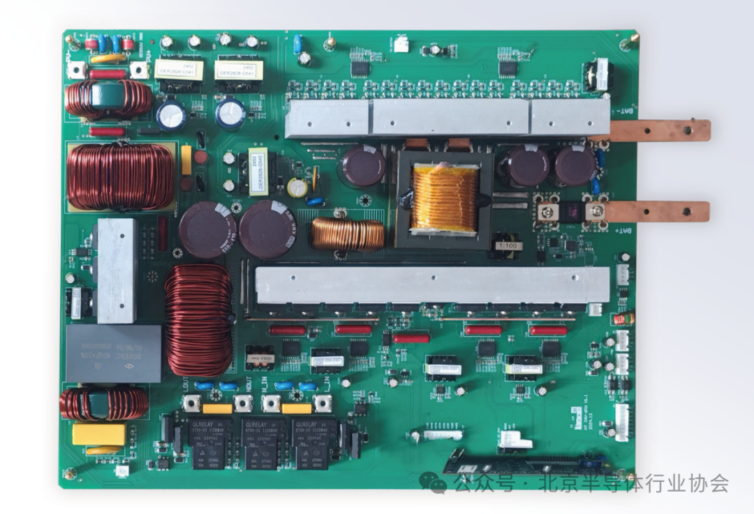
Figure 5. 6kW Household Storage System Verification Mainboard
4 Ecosystem Construction: Lowering Customer Migration Barriers
Beyond technical verification, the company alleviates customer concerns by building a “soft and hard collaborative” ecosystem: Toolchain compatibility: Providing support for third-party tools such as Keil/IAR, while also developing an equivalent CPS integrated development environment that supports debugging tools like CMSIS-DAP/JLINK. Algorithm library sharing: Open-source photovoltaic MPPT algorithms, SVPWM modulation, and other production-validated algorithm modules. Certification support: Collaborating with third-party laboratories to provide pre-certification services, shortening the product launch cycle for customers. A technical director from an inverter manufacturer commented: “The fault ride-through algorithm in the reference design can be directly migrated, helping us save 3 months of development time.” This vertical integration capability from chip to application is reshaping the competitive landscape of the market.
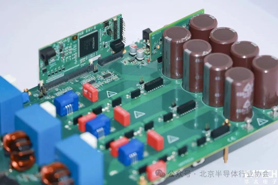
Figure 6. Inverter System DEMO Verification Mainboard
5 Market Insights: Breaking Technical Trust with System Thinking
This verification practice indicates that for domestic chip companies to achieve market breakthroughs, they must shift from the traditional mindset of selling chips to constructing a value closed loop from the perspective of customer systems. By independently building a complete application system, not only can chip performance be deeply verified, but more importantly, reusable technical solutions can be established, reducing customer replacement costs. When technical parameters translate into visible gains in power generation and measurable reductions in failure rates, market trust is naturally established.
Looking ahead, with the development of the energy Internet of Things, MCU chips will carry more intelligent diagnostics and edge computing functions. Huatai’s SOC product line plans to expand the verification system into the digital twin field, validating the adaptability of chips in new topological structures through virtual power station simulations in advance. This iterative model of “promoting research through use” may provide a new paradigm for the advanced development of domestic chips.
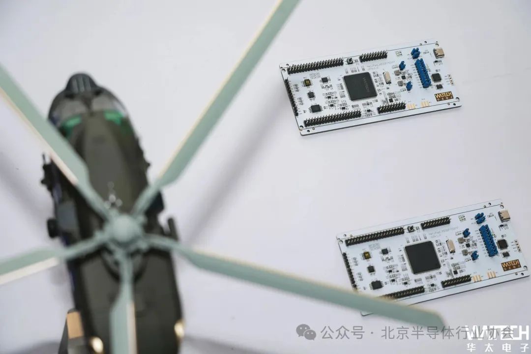
Figure 7. System Verification Control Board
Conclusion: In the arena of industrial control chips, performance parameters are merely the entry ticket; the real competition lies in the deep understanding of application scenarios and the ability to deliver value. Through empirical evidence from inverter systems, Huatai Electronics has not only validated the technical strength of the dual-core M7 chip but, more importantly, has built a trust bridge from silicon to system. This technology confidence based on vertical integration is key to breaking market monopolies and achieving domestic substitution.