AMD announced late Monday that it has achieved its first 2nm chip, which is the core complex die of its 6th generation EPYC “Venice” processor (core complex die (CPU)), and this processor is expected to launch next year.
The “Venice” core complex die is the industry’s first high-performance computing (HPC) central processing unit design that has been tape-out using TSMC’s N2 process technology, highlighting AMD’s aggressive development roadmap and the maturity of TSMC’s production nodes.
AMD’s 6th generation EPYC “Venice” processor is expected to be based on the company’s Zen 6 microarchitecture and is anticipated to launch sometime in 2026. This CPU will rely on the core complex die produced using TSMC’s N2 (2nm) manufacturing process, so it is reasonable that AMD has now received the first batch of the “Venice” core complex die produced from the factory.
Currently, AMD has not discussed the details of its EPYC “Venice” processor or core complex die, but the company’s press release states that the chip has completed tape-out and successfully powered on, which means that the core complex die has successfully been energized and passed basic functionality tests and validation.
Dr. Lisa Su, CEO of AMD, stated: “For many years, TSMC has been our key partner, and our deep collaboration with their R&D and manufacturing teams has enabled AMD to continuously deliver industry-leading products that push the limits of high-performance computing. As a major HPC customer of TSMC’s N2 process and TSMC’s Arizona Fab 21, this showcases how we work closely together to drive innovation and deliver advanced technologies that will power future computing.”
TSMC’s N2 process is the company’s first technology to use gate-all-around (GAA) nanosheet transistors. The company expects that compared to the previous generation N3 (3nm) process, its manufacturing technology will achieve a power reduction of 24% to 35%, or a performance increase of 15% at the same voltage, while increasing transistor density by 1.15 times. These improvements are primarily due to the new transistors and the N2 process’s flexible (NanoFlex) design technology that optimizes the framework.
Before AMD announced this news, its main competitor Intel delayed the launch of its next-generation Xeon “Clearwater Forest” processor, which is produced using the 18A manufacturing technology, to the first half of next year (Intel’s 18A technology aims to compete with TSMC’s N2 process).
Additionally, AMD also announced that it has successfully validated chips of the 5th generation EPYC processors produced by TSMC at its Fab 21 in Phoenix, Arizona, USA. Therefore, some of the current 5th generation EPYC CPUs can now be produced in the United States.
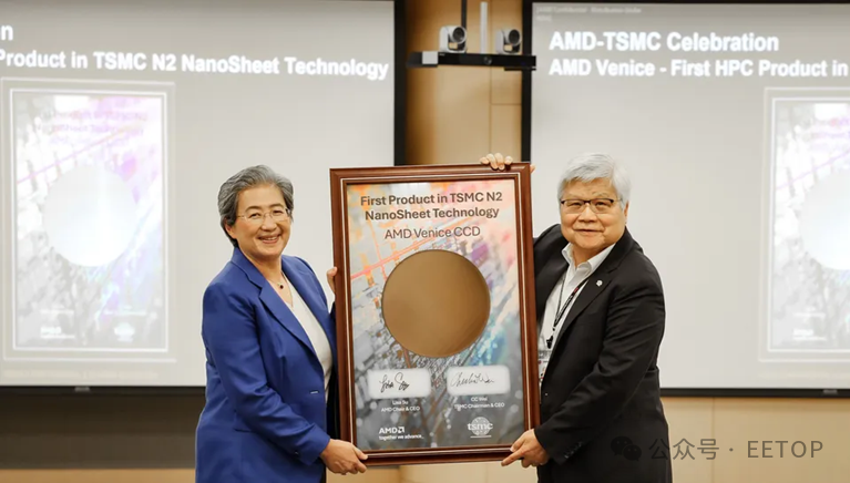
Dr. C. C. Wei, CEO and Chairman of TSMC, stated: “We are proud that AMD can be our major high-performance computing customer for our advanced 2nm (N2) process technology and TSMC’s Arizona factory. Through our joint efforts, we are driving significant technological upgrades that bring better performance, higher energy efficiency, and higher yield for high-performance chips. We look forward to continuing our close collaboration with AMD to usher in a new era in computing.”
Conference Notification and Invitation
(April 16, Beijing)