
Many people may not be very familiar with smartphones, and I am one of them. Although I use one every day, I can’t really explain much about it. I just know that suddenly everyone switched to smartphones, and I had to follow suit. However, smartphones are indeed more convenient than feature phones. What makes them better? Let’s take a look at what upgrades have been made to smartphones from a hardware perspective.Feature Phones vs. SmartphonesFeature phones generally only contain a baseband chipset, also known as BP. In contrast, smartphones include both an Application Processor (AP) and a Baseband Processor (BP). The AP is responsible for executing most applications, while the BP, also known as the Communication Processor (CP), handles all communication software execution. An example of a feature phone is the LG Electronics Cyon LG-KP4000[1]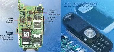 The phone supports CDMA 2000 and uses a Qualcomm chipset, which includes the Qualcomm MSM 6100. When we talk about CDMA chipsets, they are generally divided into four parts. The first part is the MSM chip, which is the baseband chip used in mobile terminals, providing modulation, demodulation, multimedia functions, etc. The other two parts are RFR and RFT, where RFR refers to the radio frequency reception part, and RFT refers to the radio frequency transmission part, together forming the RF radio frequency chip. The fourth part is the power management section. Regardless of whether it is CDMA2000 or WCDMA, wireless terminals require these four types of semiconductor products: MSM, RFR, RFT, and power management.Smartphones: AP and BPIf we say that the hardware structure of feature phones is primarily based on BP, with some additional applications and corresponding hardware peripherals, then smartphones represent a further development of feature phones. They add AP on top of BP, specifically to enhance support for applications. Most smartphones contain two processors. The operating system, user interface, and applications run on the Application Processor (AP), which typically uses an ARM chip CPU. Meanwhile, the mobile RF communication control software runs on a separate CPU known as the Baseband Processor (BP). The main reason for executing RF functions (signal modulation, encoding, RF displacement, etc.) on the BP is that these functions are highly time-sensitive. The best approach is to execute these functions on a main CPU that runs a real-time operating system. Another benefit of using BP is that once it is designed and certified, it can correctly execute its functions (communication functions) regardless of changes in the operating system and application software. Additionally, bugs in the operating system and drivers will not lead to catastrophic data being sent to the mobile network (as required by the FCC)[5]. Below is a hardware diagram of a smartphone.
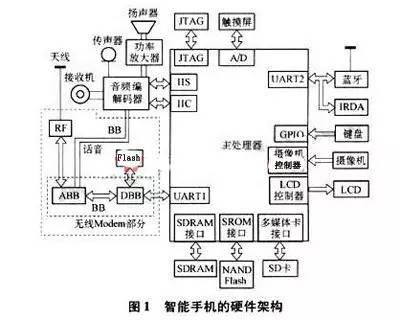 The main processor runs an open operating system and is responsible for controlling the entire system. The digital baseband chip (DBB) for the wireless modem primarily completes the A/D conversion and D/A conversion of voice signals, codec for digital voice signals, channel coding, and timing control for the wireless modem. The main and secondary processors communicate via a serial port. The BP part includes the CPU, memory, power management, wireless transceiver, power amplifier, and other components, which are essentially the original structure of feature phones. In the hardware architecture of smartphones, the wireless modem part only needs to add certain peripheral circuits, such as audio chips, LCDs, camera controllers, microphones, speakers, power amplifiers, antennas, etc., to form a complete hardware circuit of a regular mobile phone (traditional phone). The analog baseband (ABB) voice signal pins communicate with the audio codec chip, forming the voice channel during calls. Initially, the AP and BP parts were separate, communicating via AT commands. The following image[4] shows the actual motherboards of the Moto Droid and iPhone 3GS. It is important to note that the CPU chip is not visible in the physical image because the CPU and RAM are stacked together on the motherboard. This method is called Package on Package (PoP), and its main advantage is saving motherboard space.
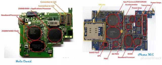 In early mobile phones, the physical connection between AP and BP was achieved through a serial port (UART), which not only required a serial port but also typically needed General Purpose Input/Output (GPIO) control lines to coordinate power management between AP and BP. When the phone is idle, both AP and BP parts are in sleep mode to save power. When making a call, the AP wakes up the BP via GPIO and then sends AT commands to the BP through the serial port. When there is an incoming call, the BP also wakes up the AP via GPIO and sends AT commands through the serial port to notify the AP to start ringing and switch the phone interface, etc. Clearly, coordinating the work of AP and BP using UART, GPIO, and AT commands is not very efficient. Although later phones replaced UART with USB or SPI, improving efficiency somewhat, overall, the coordination between AP and BP remains a bottleneck in the overall efficiency of the phone. Each of AP and BP has its own independent CPU chip, which not only results in poor communication efficiency between them but also increases the cost of purchasing chips, occupies more space on the phone’s circuit board, and consumes more power. To overcome these shortcomings, the emergence of SoC (System on Chip) integrated chips is a trend. The challenge lies in the design and manufacturing difficulty of SoC chips. For example, within the SoC, the division of labor between AP and BP remains clear, and communication between them usually relies on shared memory. However, the technical difficulty of implementing shared memory is much more complex than using AT commands. For some newer manufacturers, such as tablets and e-readers, BP modules are used.Examples of SmartphonesThe GPhone Nexus One uses Qualcomm’s QSD8250, and the G1 and G2 use Qualcomm’s MSM7200 chip, both of which are SoC chips that integrate AP and BP. Taking the MSM7200 chip as an example, its AP part contains two CPU cores, one ARM11 and another DSP dedicated core QDSP5, while the BP part also has two CPU cores, ARM926 and DSP dedicated core QDSP4. The CPU chip built into the GPhone Nexus One is Qualcomm’s Snapdragon series QSD 8250 chip, with an ARM Cortex-A8 core. Qualcomm’s MSM6xxx series are baseband chips, and the MSM7xxx series are AP+BP SoC chips that were gradually released around 2006. There are three main approaches for BP: 1. Discrete components, which were the primary implementation method for the BP part of early smartphones, such as phones using Intel PXA series chips as CPUs. Currently, iPhone, Palm Pre, and Moto Droid also follow the discrete component structure. 2. BP modules, which are simple to use but costly. This design is commonly used in non-phone mobile devices. 3. AP+BP integrated SoC chips, which have the highest technical difficulty but also the highest profit margins, are currently the most commonly used BP implementation method in phones. For example, HTC phones use both TI’s SoC chips and Qualcomm’s SoC chips, while most Nokia smartphones use TI’s SoC.Mobile Phone Manufacturing ProcessThe mobile phone design and development process can be divided into the following six steps. Step 1 The Design House obtains reference designs from chip manufacturers. The reference designs provided by chip manufacturers often come in the form of development boards, which are much larger than mobile phones, with some boards even comparable in size to newspapers. The image shows Samsung’s S3C44BOX chip development board. Step 2 Determine the components. 1. Mainboard design, either Gerber files or PCB boards. 2. System software. 3. A complete list of components to be assembled (BOM List). 4. Matching casing. Step 3 Develop and debug drivers. Step 4 Product-level mainboard design. After determining the microprocessor chip and components, the Design House begins to convert the large board into a small board, which is the design of the product-level mainboard. The product-level mainboard design aims to make the mainboard more compact, including layout and wiring, while adding fasteners, insulation, and heat dissipation materials to make the phone more durable. Step 5 Further debug the hardware and software to reach product level. Step 6 The Design House designs some reference casings and presents the complete design from inside to outside to the manufacturers.
Follow us