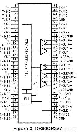
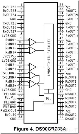
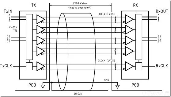
Currently, digital video in circuits uses the Camera Link interface for transmission. The previous solution involved the FPGA outputting parallel data signals along with synchronization control signals, which were then processed by the serializer chip DS90CR287 to convert parallel to serial. After processing, the output was sent through the Camera Link interface, with the capture card using DS90CR288 for the same conversion. This method consumes a lot of FPGA pin resources. When transmitting 24-bit RGB signals, it requires 24 (signals) + 4 (synchronization control) + 1 (clock) = 29 pins. However, using LVDS transmission with the altlvds_tx core only requires 5 pairs of LVDS signals, occupying a total of 10 pins.
LVDS transmission lines are twisted pairs.
Now, many serial AD converters have appeared on the market, and with multiple channels, the altlvds_rx core can be used to receive data. It makes me feel embarrassed to think that my own designed board still has multiple parallel ADs! When multiple ADs are needed in a circuit, using parallel ADs results in a larger board size and consumes more FPGA pins. In contrast, using multi-channel (dual-channel, quad-channel, octal-channel) serial ADs can significantly reduce board size and save FPGA pin resources. In future designs, I will try to use such chips as much as possible.
I am preparing to design a circuit that uses the FPGA LVDS interface to transmit Camera Link video signals. The front-end detector outputs 4 analog signals, which are quantized using 4 parallel ADs, processed by the FPGA, and then output as LVDS signals through the LVDS interface using the altlvds_tx core. This work is part of my graduation project… I plan to write a series on the use of LVDS in FPGA to document and share the design process.
First, let me introduce the origin of LVDS. LVDS stands for Low-Voltage Differential Signaling, a signal transmission mode proposed in 1994 by National Semiconductor (now acquired by TI). It is a voltage level standard aimed at overcoming the disadvantages of high power consumption and significant EMI (electromagnetic interference) when transmitting broadband high bit-rate data using TTL levels. The LVDS output interface transmits data through differential signaling on two PCB traces or a pair of balanced cables, utilizing a very low voltage swing (approximately 350mV). By adopting the LVDS output interface, signals can be transmitted at rates of hundreds of Mbit/s over differential PCB lines or balanced cables. Due to the use of low voltage and low current drive methods, it achieves low noise and low power consumption.