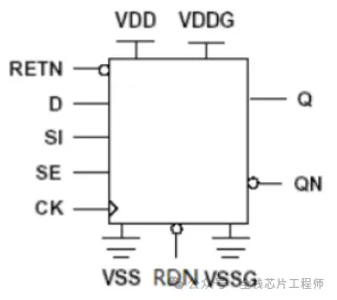
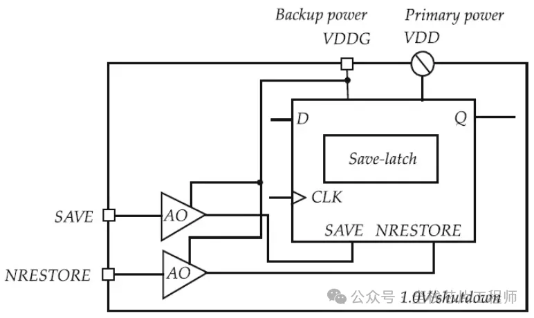
The retention cell can maintain its internal state even when the primary power supply VDD is turned off, but it is not completely powered down; there is still a backup VDDG power supply.
2) RETN Control Signal
Who decides the power supply for RETN? Can RETN be powered off?
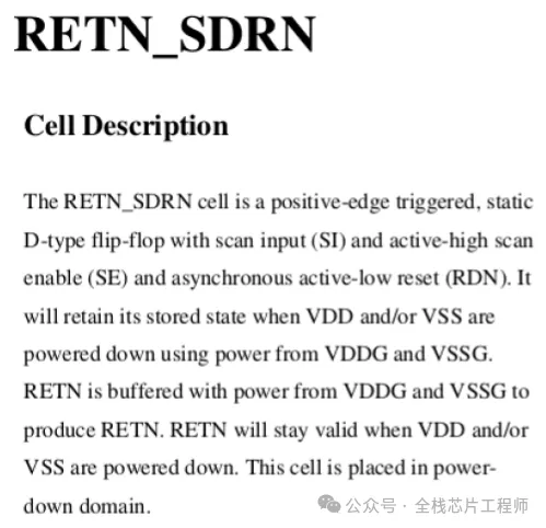
Answer: RETN is driven by BUF, which is powered by VDDG and VSSG. After VDD and VSS are powered off, RETN needs to remain valid, specifically designed by the PMU module. Jingxin SoC provides PMU design. Note that Jingxin SoC places the RETN signal in the power shut power domain to minimize the use of always-on buffers. The reasons for reducing the use of always-on buffers have been discussed extensively in the Jingxin SoC training camp and will not be elaborated further.
Note that the save-latch is generally a high-voltage threshold (HVT) cell to save static power, and the save-latch is powered by the backup power supply VDDG and VSSG.
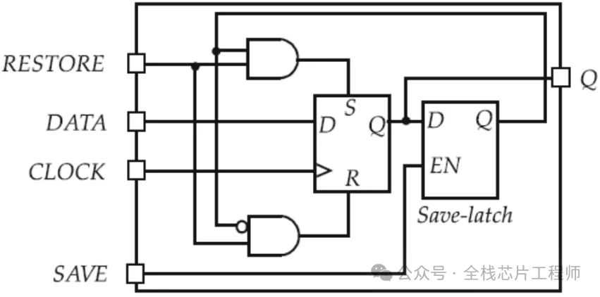
Under normal conditions, the retention flip-flop functions like a normal flip-flop but will store the output in the save-latch when the SAVE signal is valid. When the power is turned off, the save-latch retains the signal saved by SAVE since it is powered by the backup power supply. When the RESTORE signal is pulled high, the save-latch quickly sends the output back to the preceding flip-flop, restoring the state from power-off, similar to how a web browser automatically reopens tabs after closing, providing a smooth experience.
Can retention cells be used extensively? What are the implications of extensive use? Are there good solutions? Can the design solutions of Jingxin SoC eliminate the drawbacks of retention cells? We welcome everyone to discuss in the full-stack chip engineer knowledge community.
Chip Full Process Training
Chip Training is about to increase in price, please sign up contact the editor via WeChat: 13541390811
-
Jingxin SoC front-end, mid-end, and back-end low-power full process practical training(Price is less than 1/6 of peers)
-
Jingxin SoC front-end video + documents + practical experience + one-on-one lifelong guidance practical training
-
Jingxin SoC mid-end video + documents + practical experience + one-on-one lifelong guidance practical training
-
Jingxin SoC back-end video + documents + practical experience + one-on-one lifelong guidance practical training
-
12nm 2.5GHz A72 low-power DVFS practical training(Price is less than 1/3 of peers)
-
12nm 2.5GHz A72 DFT practical training(Price is less than 1/3 of peers)
-
RISC-V MCU 40nm full chip PR practical training
-
DDR4/3 project practical training
-
MIPI CSI2 + ISP image processing + HDMI practical training (i.e., Jingxin SoC front-end)
-
MIPI CSI2 + ISP image processing + H.265 + USB + MAC practical training (in development)
-
Advanced Codec H.265/H.264 practical training (in development)
Introduction to Chip Design Service:
-
Providing SoC, MCU, ISP, CIS chip design, verification, DFT design services
-
Providing DDR/PCIE/MIPI/CAN/USB/ETH/QSPI/UART/I2C IP design
-
Providing backend design for processes including 7nm, 12nm, 28nm, 40nm, 55nm, 65nm, 90nm
-
Providing customized chip design services and training for universities and enterprises, as well as employment recommendations and guidance
In addition, the editor shares knowledge about chip design, verification, DFT, and backend full process knowledge along with a large number of technical documents in the knowledge community. Everyone is welcome to join the discussion and learn together!

[Enable every student to design an SoC/MCU chip]
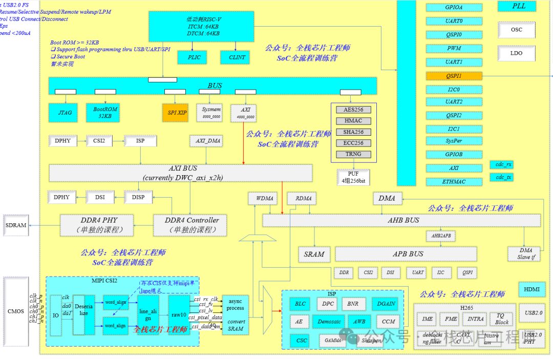
[The only one on the internet] Jingxin SoC is a low-power ISP image processing SoC used for [chip full process design training], employing a low-power RISC-V processor, with ITCM SRAM and DTCM SRAM built-in, integrated with IPs including MIPI, ISP, USB, QSPI, UART, I2C, GPIO, Ethernet MAC controller, etc., and designed using SMIC40 process.
-
High-speed interface Verilog design implementation -
From image algorithms to RTL design implementation -
MIPI, ISP Verilog implementation and simulation -
Lint, CDC checks, and UVM verification -
Post-simulation
The content of just the front-end course is worth 5-6 courses from other training institutions.
-
DFT design (chip-level) -
Synthesis logic synthesis (chip-level) -
Low power UPF design, CLP technology -
Formal verification and other technologies
(3) In the SoC back-end course, you will learn
-
Low power design
-
Layout and routing (low power FF flow) -
StarRC/QRC -
STA/Tempus -
Power analysis -
DRC/LVS design
The content of just the back-end course is worth 3-4 courses from other training institutions.
Join the knowledge community and become part of the chip design knowledge repository!
Knowledge Community of SoC Training Camp

SoC training camp VIP students ask why the low power cell is not inserted into the netlist?
While asking questions is encouraged, when faced with problems, we should first think proactively and try to solve them. If we really cannot solve them, then we can seek help. This way, we grow faster.
First, when I received this question, I opened the log. Checking the log is a virtue in IC design! I found that the EDA tool reported a warning after ingesting the UPF file, indicating that many FF libraries were used.
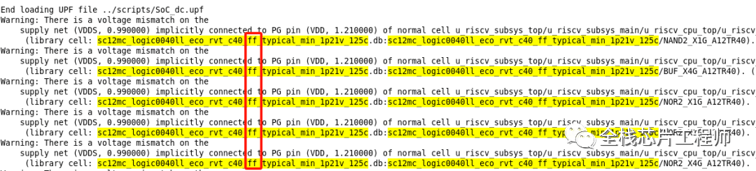
The error indicated that the UPF specified a voltage of 0.99V, while the CELL was 1.20V. The voltage mismatch resulted in the logic synthesis not inserting the MV CELL. Note that during synthesis, we used the SS library, so why would it be using the FF library? I opened the constraint script and found the following bug:
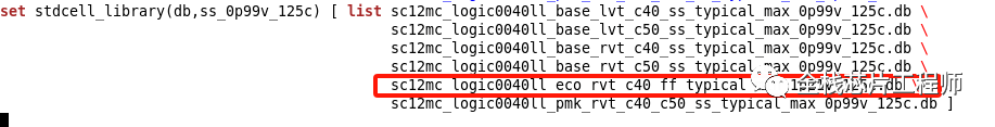
So, I changed the constraint to replace FF with SS. After running again, the results came out:
In the low power design section, I will leave a small bug inside the design, which is very simple. I will not disclose the answer. Everyone must think more and run the simulations; this way, you will learn deeply.
Training students please note that Jingxin SoC uses the always-on power domain voltage domain’s pwrdown_mux signal as the switch control signal for the power switch cell. However, there is a small issue in the design that is not exactly a bug, but for the UPF low power flow, it is undoubtedly a bug!
Training students please log in to the server to track the pwrdown signal and pay attention to its load conditions. The RTL code is as follows:

Combining the PR output netlist, we will conduct a CLP low power check. The script can be found on the server. It can be found that the CLP reports an error stating that the switch control signal for the power switch is not found.

It must be said that CLP checking is extremely important for low power and for chip design! The value of Jingxin SoC lies in connecting all these small knowledge points of the chip design full process! What are you waiting for? Hurry up and sign up!
During the mid-process of chip design, Jingxin SoC will insert isolation and other cells from the UPF constraints, but it cannot insert power switch cells. Therefore, the control signal pwrdown_mux for the power switch cell, when there is no load, will be optimized away (removed). Therefore, it is necessary to set the above MUX device as dont_touch or make pwrdown_mux a module port and prohibit auto_ungroup (and set no_boundary_optimization), so that this signal can be retained for the backend to implement power switch control. Please students complete the code modification and complete the following tasks based on the full set of flow environment:
-
Lint check, front-end simulation,
-
Complete mid-end and back-end flow,
-
Complete CLP check, complete post-simulation
In the 7-day sprint PR training camp, some students asked why the same floorplan had some students run through quickly while others encountered numerous DRC issues (EDA tools iterating continuously) preventing the tools from completing. What exactly is the problem?
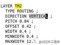
First, I found that the student defined TM2 as horizontal, while those familiar with Jingxin technology know that the preference direction for TM2 is VERTICAL.
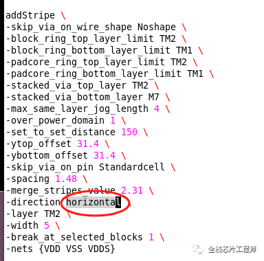
Checking the Jingxin LEF library file can also confirm:
What impact does using the wrong direction have? Everyone should practice with Jingxin SoC’s back-end flow to find out the truth.
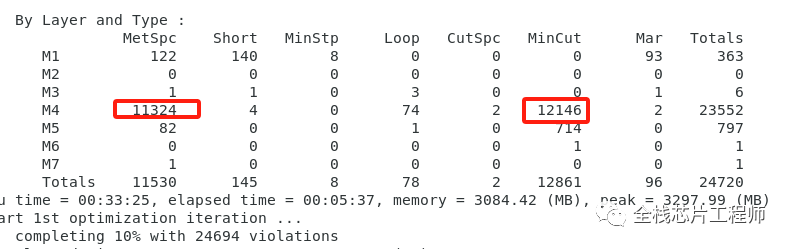
In the 7-day sprint PR training camp, some students asked why the PR took a full day and night (24 hours) to complete routing but still had numerous DRC errors? I have minimized the design scale to speed up PR design, and in reality, it can be completed in 2 hours, so why so slow? The reason is the routing of low power units. The specific reasons and solutions are welcome to discuss in the Jingxin training camp.
The errors are mainly concentrated on M4; please think about how to solve this.
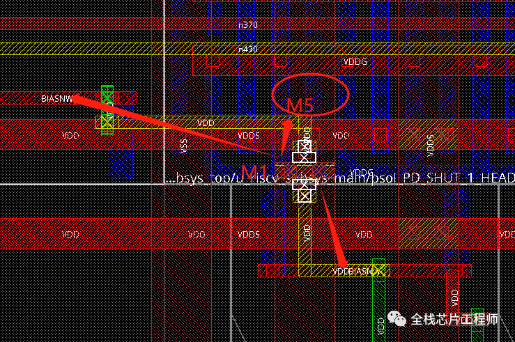
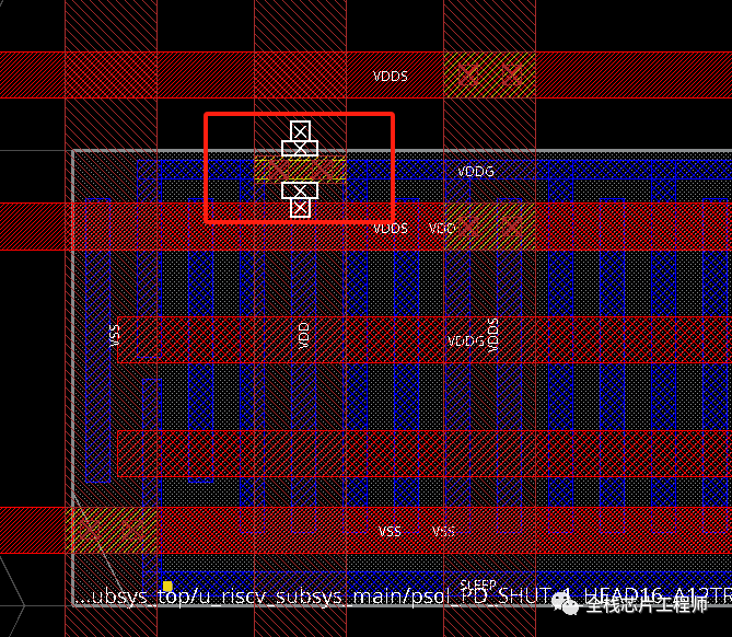
In the 7-day sprint PR training camp, some students asked why the second PG pin (VDDG) of the power switch cell is connected from M1 instead of M2. Please think about what the problem is and how to solve it.
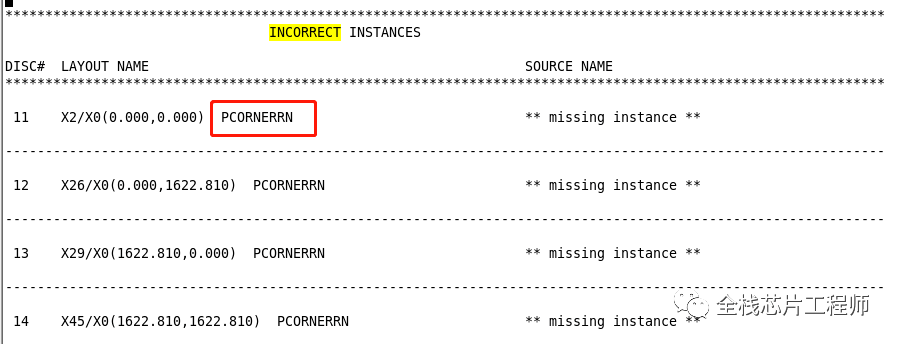
In the 7-day sprint PR training camp, some students asked how to handle LVS issues with corner pads not passing?
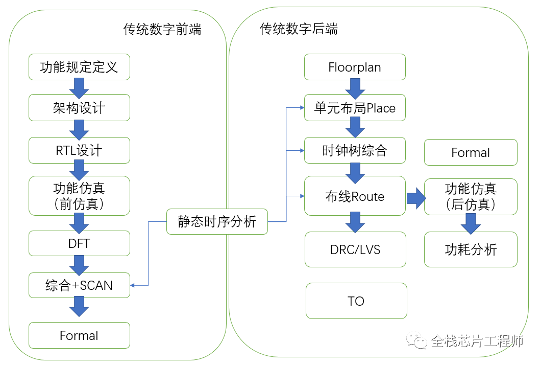
After completing the front-end design simulation and DFT of Jingxin SoC training, we arrive at the back-end flow. This tutorial teaches you how to run the digital back-end flow in one click.
The script command to generate is as follows:
tclsh ./SCRIPTS/gen_flow.tcl -m flat all
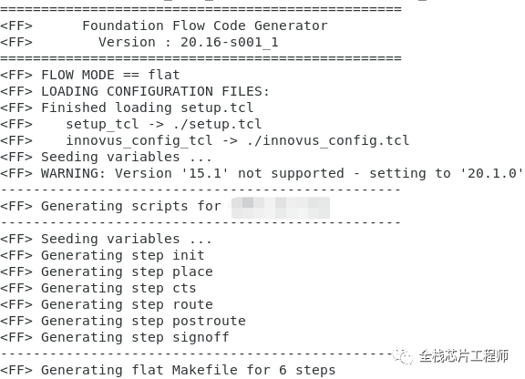
Before generating the flow script, it is necessary to configure related parameters in setup.tcl, etc. Please refer to the [the only one on the internet] [full-stack chip engineer] providing self-developed Jingxin SoC front-end engineering, DFT engineering, and back-end engineering to guide you through the entire process of participating in SoC project design from algorithm, front-end, DFT to back-end.
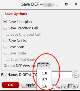
Students in the Jingxin SoC training camp asked why Innovus reports an error when reading the completed floorplan def file? First, check the log:
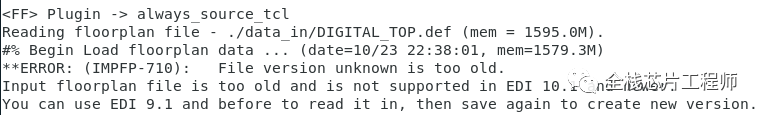
Reading floorplan file – ./data_in/DIGITAL_TOP.def (mem = 1595.0M).
#% Begin Load floorplan data … (date=10/23 22:38:01, mem=1579.3M)
**ERROR: (IMPFP-710): File version unknown is too old.
In the past EDI era, we could load the floorplan by defining fp_file:
set vars(fp_file) “./data_in/DIGITAL_TOP.def”
However, Innovus has upgraded and abandoned the fp_file loading method. Of course, we can use the old version of EDI 9.1 and earlier to add fp_file and then save it to create a new version, but this is clearly unnecessary. As indicated in the log, checking the log is a very good engineering habit.
Input floorplan file is too old and is not supported in EDI 10.1 and newer.
You can use EDI 9.1 and before to read it in, then save again to create a new version.
My intuition tells me to check which DEF version the student saved the file in?
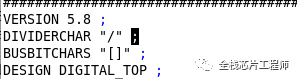
The student’s saving method is as follows:
So how to solve it? Please join the Jingxin training camp for practice.
Jingxin SoC uses many asynchronous FIFOs. Students interested in asynchronous RTL implementation can extract the asynchronous FIFO to observe the layout wiring:
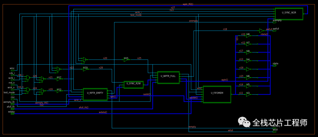
Check the area of all asynchronous FIFO cells;
dbget [dbget top.insts.pstatus unplaced -p].area
Check the names of all asynchronous FIFO cells:
dbget [dbget top.insts.pstatus unplaced -p].name
So how to extract asynchronous paths to observe layout routing? How to report timing? More content can be found in the knowledge community and SoC training camp.
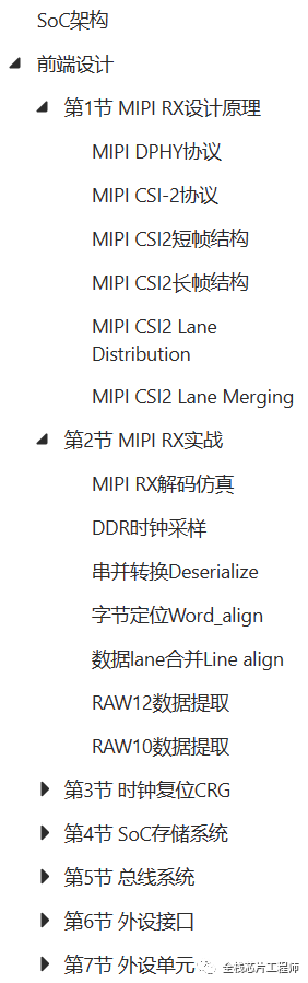
Front-End Design Directory
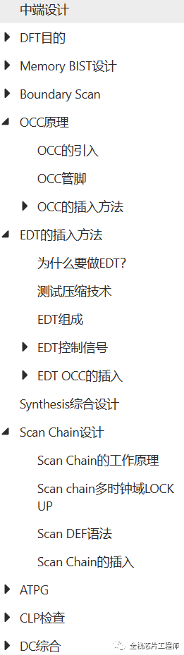
Mid-End Design Directory
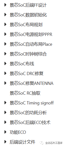
Back-End Design Directory
Welcome to join the [full-stack chip engineer] knowledge community to exchange technology and share insights from algorithm, front-end, DFT to back-end design.Click the image below to join the knowledge community!

Welcome to join the SoC MCU full process design exchange group, first add me on WeChat, and after verifying your position, you can join the group!
SoC MCU full process design group 4
SoC MCU full process design group 3
SoC MCU full process design group 2
SoC MCU full process design group 1
Welcome to join the CMOS image sensor + ISP group, first add me on WeChat, verify your position, and then join the group!
CMOS image sensor + ISP group 2
CMOS image sensor + ISP group 1