Power Consumption in CMOS Circuits is Divided into Two Parts: Static Power Consumption and Dynamic Power Consumption;
Static power consumption is caused by leakage current; dynamic power consumption is divided into switching power and short-circuit power. Switching power is the power consumed during the transition from 0 to 1, while short-circuit power occurs when both PMOS and NMOS are conducting.
The most effective method for low power consumption is: turning off the power supply. Previously, I introduced low power design in SoC—isolation, and today I will introduce the power switch cell.
No matter how low the voltage, how low the clock frequency, or how small the leakage library, it is not as thorough as completely turning off the voltage of certain functional modules. Of course, the addition of power-gating significantly increases design complexity, requiring a complete process/system methodology support from architecture design, RTL, verification, DFT, backend implementation to signoff.
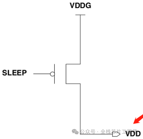
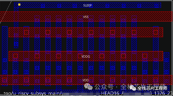
Power switch cells are divided into HEAD type and FOOT type:
HEAD Type:
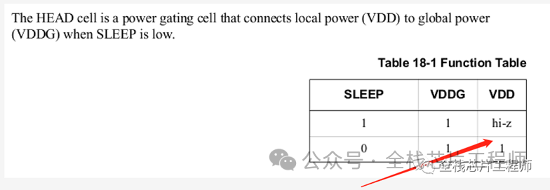
When SLEEP is 1, VDD is turned off.
When SLEEP is 0, VDD is turned on.
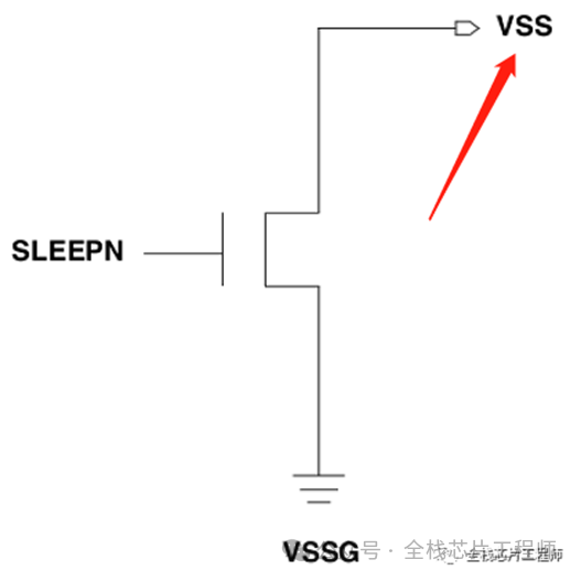
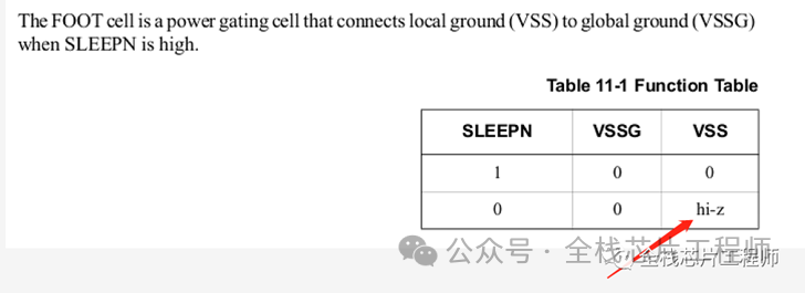
FOOT Type:
HEAD type turns off VDD, while FOOT type turns off VSS, which is rarely used.
As seen in the images above, the power switch cell is composed of PMOS/NMOS transistors. Unlike the contact switches in high-power circuits, a strong electrical switch can provide a very large current to switch the circuit, but a MOS transistor has very limited driving capability. Therefore, a SoC chip will use a large number of power switch cells, and the number of required power switch cells needs to be calculated based on design current, power switch cell driving current, and other parameters.
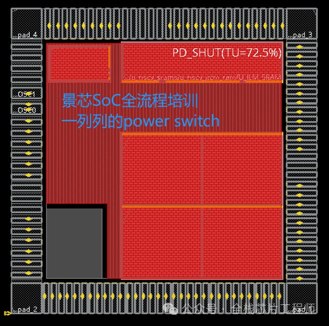
Generally, power switch cells are placed in rows just like standard cells. The upper metal layer of the power supply connects to the input terminal VDDG (VDD Global) of the power switch cell, while the output terminal connects to the power rail. The SLEEP signal acts as an enable signal, controlling the disconnection/connection of the rail and the upper metal to achieve power shutdown.
How exactly are they connected? For specific connections, please refer to the knowledge community.
Jingxin SoC Full Process Training, some students encountered the following issues with the power switch:
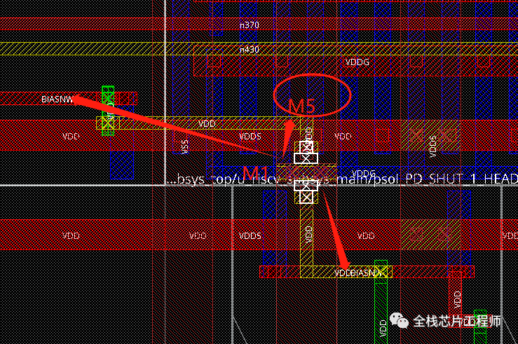
The secondaryPowerPin of the power switch is the VDD shown in the image below (connected to the power VDDS), and the VDDG pin of the power switch connects to the input voltage VDD of the power switch. During the backend implementation of Jingxin SoC, it was found that the secondaryPowerPin always connects to M1 when connecting to the power stripe (M5), rather than the red M2 metal.
As shown: the secondaryPowerPin always connects to M1 when connecting to the power stripe (M5), rather than the red M2 metal.
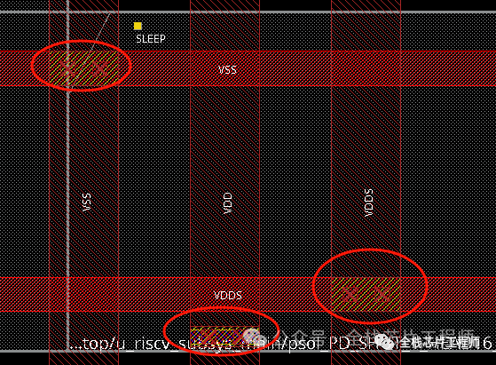
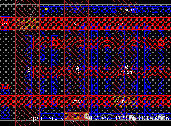
Opening CELL visibility reveals that the stripe in the middle is VDD and is connected to M1 (blue). Why is it connected to M1 instead of M2 (red)?
For specific reasons, please refer to the knowledge community.
[To Enable Every Student to Design an SoC/MCU Chip]
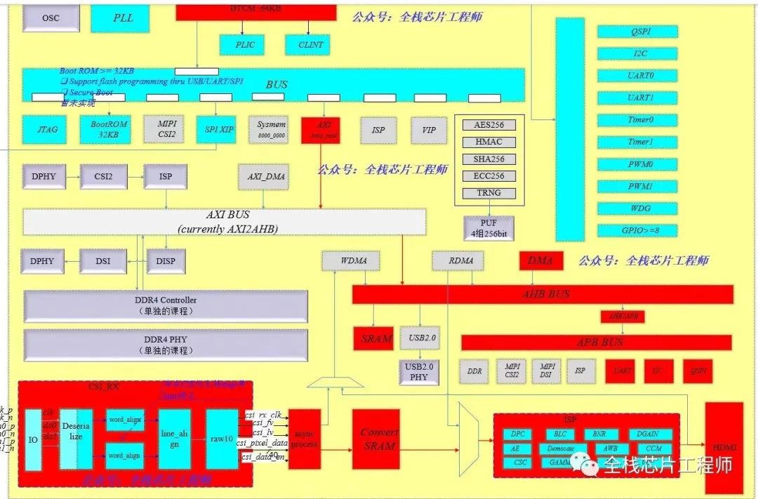
[The Only One] Jingxin SoC is a low-power ISP image processing SoC used for [Chip Full Process Design Training], using a low-power RISC-V processor, with built-in ITCM SRAM, DTCM SRAM, and integrates IPs including MIPI, ISP, USB, QSPI, UART, I2C, GPIO, Ethernet MAC controller, etc., designed using SMIC40 process.
-
High-speed Interface Verilog Design Implementation -
Image Algorithm and Verilog Design Implementation -
MIPI Communication Protocol Verilog Implementation -
Lint, CDC Checks and UVM Verification -
Post-simulation
The content of just the frontend course is equivalent to 5-6 courses from other training institutions.
-
DFT Design (Chip Level) -
Synthesis Logic Synthesis (Chip Level) -
Low Power UPF Design, CLP Technology -
Formal Verification and Other Techniques
(3) In the SoC Backend Course, You Will Learn
-
Low Power Design
-
Layout and Wiring (Low Power FF Flow) -
StarRC/QRC -
STA/Tempus -
Power Analysis -
DRC/LVS Design
The content of just the backend course is equivalent to 3-4 courses from other training institutions.
The course provides servers for everyone to practice! It takes you through the entire process from algorithms, frontend, DFT to backend in SoC project design.Please contact the author to register! Contact WeChat: 135-4139-0811
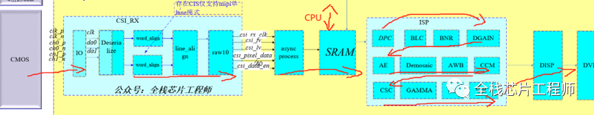
The data path of the Jingxin SoC training camp for image processing:
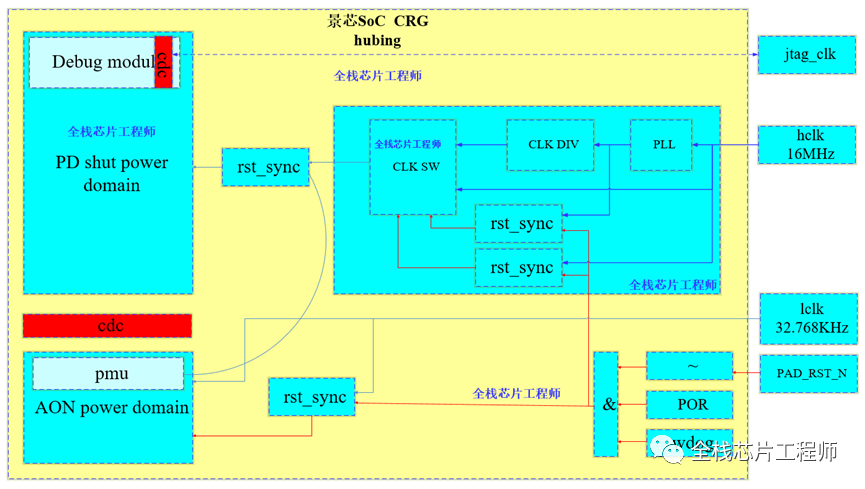
The CRG design of the Jingxin SoC:
Join the knowledge community and become part of the chip design knowledge treasure!
The Knowledge Community of the SoC Training Camp
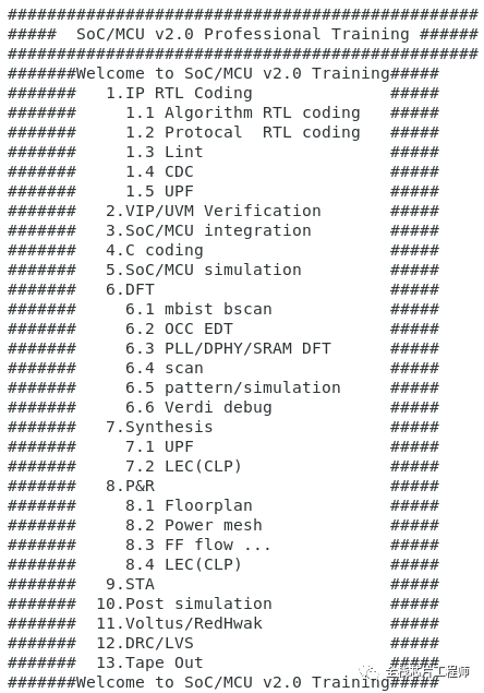
One-click completion of C code compilation, simulation, synthesis, DFT insertion, formal verification, layout and wiring, parasitic parameter extraction, STA analysis, DRC/LVS, post-simulation, formal verification, power analysis, etc. The upgraded chip design engineer V2.0 flow is as follows:
SoC One-Click Execution Flow
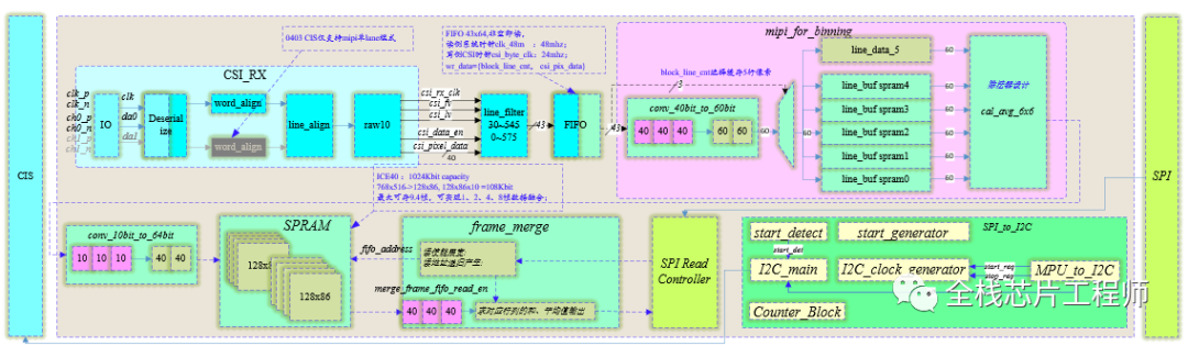
MIPI DPHY + CSI2 Decoding
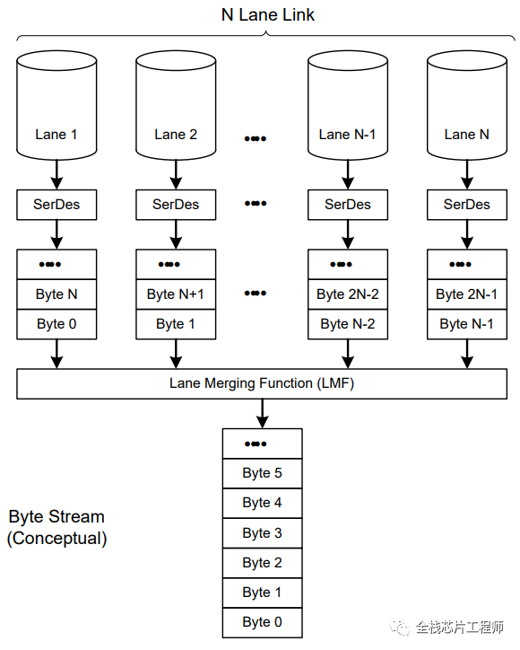
Classic Design in Digital Circuits: Implementation of Multiple Communication Data Lane Merging
Classic Design in Digital Circuits: Implementation of Multiple Communication Data Lane Distribution
UPF Low Power Design
Full Chip UPF Low Power Design (Including DFT Design)
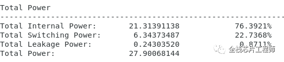
The Jingxin SoC training camp training project, before low power design, the power consumption was 27.9mW.
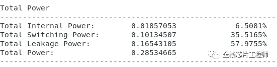
After low power design, the power consumption is 0.285mW, a reduction of 98.9%!
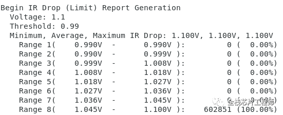
Voltage Drop Check:
Low Power Check:
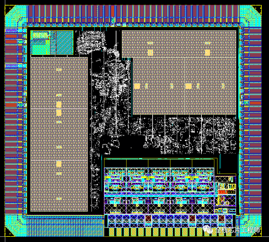
Chip Layout Design V1.0
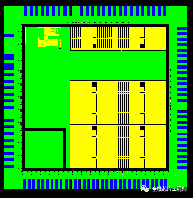
Chip Layout Design V2.0
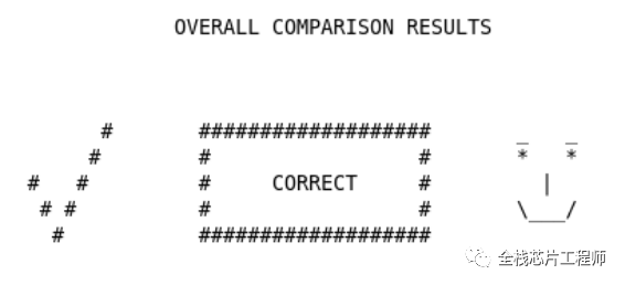
DRC/LVS of low power design, the LVS practice of the chip’s top layer is extremely valuable and challenging! Unique experience sharing in the industry.
ISP Image Processing
-
dpc – Bad Pixel Correction

-
blc – Black Level Correction

-
bnr – Bayer Noise Reduction
-
dgain – Digital Gain
-

-
demosaic – Demosaicing

-
wb – White Balance Gain
-
ccm – Color Correction Matrix
-
csc – Color Space Conversion (Integer Optimized RGB2YUV Conversion Formula)
-
gamma – Gamma Correction (Brightness Based on Table Lookup Gamma Correction)
-
ee – Edge Enhancement

-
stat_ae – Auto Exposure Statistics
-
stat_awb – Auto White Balance Statistics
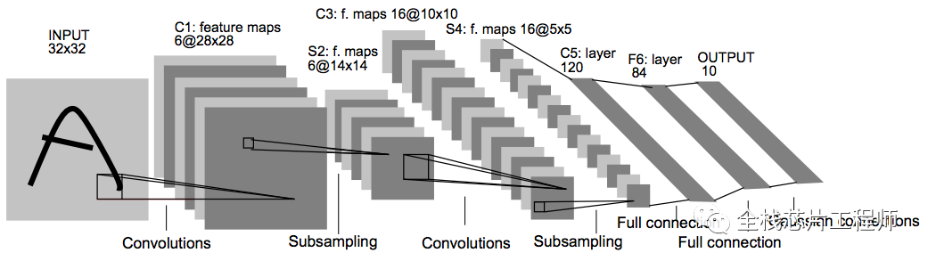
CNN Image Recognition
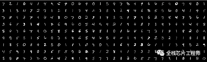
Support for Handwritten Digit AI Recognition:
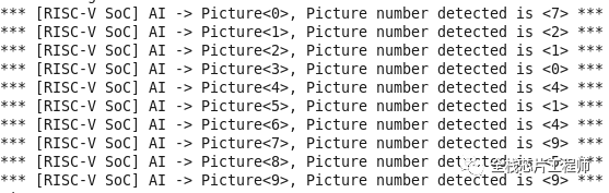
Simulation Results: Simulated Recognition of Digits 7, 2, 1, 0, 4, 1, 4, 9
Jingxin Micro SoC Team Business
Introduction to the Jingxin Micro SoC Team Business:
-
Providing the most comprehensive actual chip project training online
-
Providing SoC, MCU, ISP, CIS chip design services
-
Providing chip design, verification, DFT design services
-
Providing backend design services, processes including 7nm, 12nm, 28nm, 40nm, 55nm, 65nm, 90nm, 110nm, 180nm, etc., providing wafer fabrication channels
-
Providing customized chip design training for universities and enterprises, as well as job recommendations and guidance
Rich Tutorial Documentation
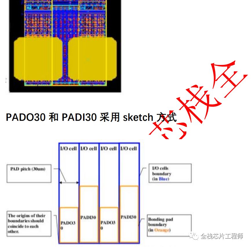
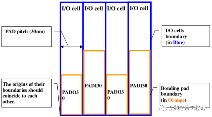
In the 7-day sprint PR training camp, students ask how to add PAD to IO? Please think about how to achieve the best IO and PAD for Jingxin SoC?
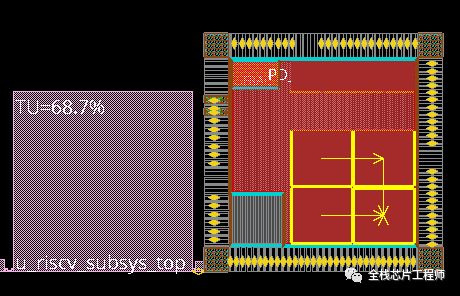
In the 7-day sprint PR training camp, students ask why it took 24 hours to complete the routing with the same floorplan but encountered a large number of DRC issues (EDA tools continuously iterating), causing the tools to never finish running. What is the specific problem?
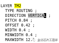
First, I found that the student’s stripe defined TM2 as horizontal, while those familiar with the Jingxin process know that the preference direction of TM2 is VERTICAL.
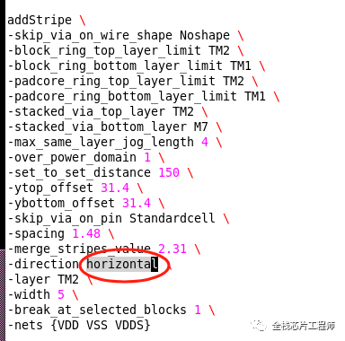
Checking Jingxin’s LEF library file can also confirm:
What impact does using the wrong direction have? Everyone should practice with Jingxin SoC’s backend flow to gain practical knowledge.
In the 7-day sprint PR training camp, a student asked why PR took a whole day and night (24 hours) to complete the wiring but still had a large number of DRC errors? I have minimized the design scale to speed up PR design; in fact, routing can be completed in 2 hours. Why is it so slow? The reason is the routing of low power units. For specific reasons and solutions, feel free to join the Jingxin training camp for discussion.
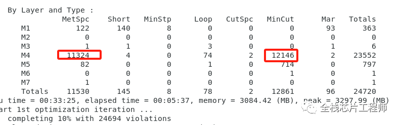
The errors are mainly concentrated on M4. Please think about how to solve this.
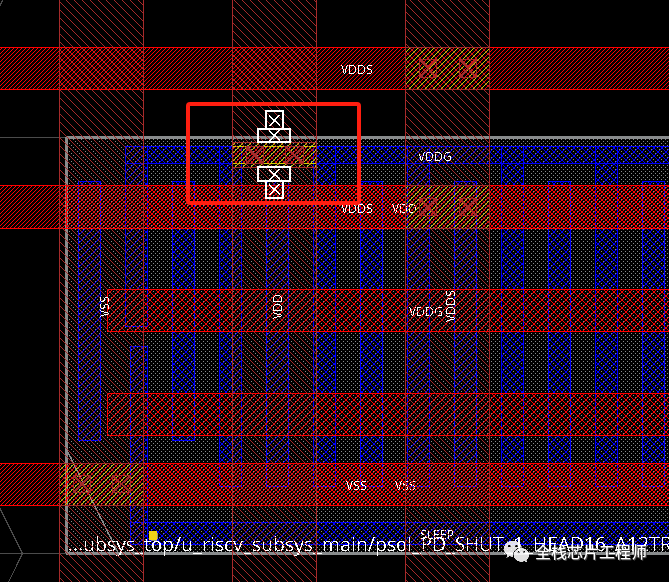
In the 7-day sprint PR training camp, a student asked why the second PG pin (VDDG) of the power switch cell is connected to M1 instead of M2. What could be the problem? How to solve it?
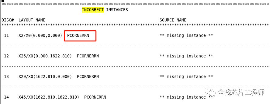
In the 7-day sprint PR training camp, a student asked how to handle Corner Pad LVS failures encountered in the Jingxin SoC training camp?
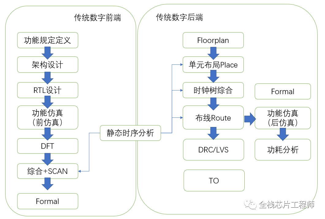
After completing the frontend design simulation and DFT in the Jingxin SoC training, we move on to the backend flow. This tutorial teaches you how to run the digital backend flow in one click.
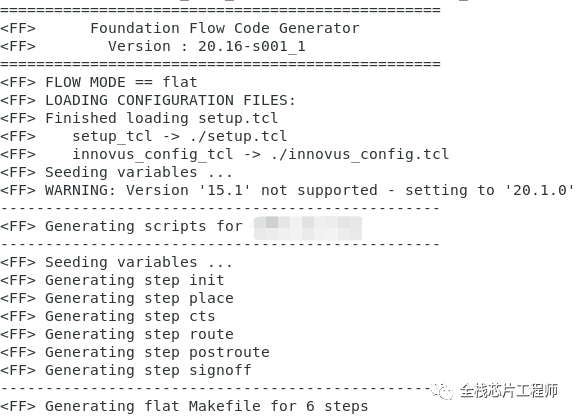
The command to generate the script is as follows:
tclsh ./SCRIPTS/gen_flow.tcl -m flat all
Before generating the flow script, relevant parameters like setup.tcl need to be configured. For specifics, please refer to the [Only One] [Full Stack Chip Engineer] who provides self-developed Jingxin SoC frontend engineering, DFT engineering, and backend engineering, guiding you through the entire process from algorithms, frontend, DFT to backend in SoC project design.
Students in the Jingxin SoC training camp ask why Innovus reports an error when reading the completed floorplan def file? First, check the log:
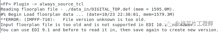
Reading floorplan file – ./data_in/DIGITAL_TOP.def (mem = 1595.0M).
#% Begin Load floorplan data … (date=10/23 22:38:01, mem=1579.3M)
**ERROR: (IMPFP-710): File version unknown is too old.
In the past EDI period, we could load the floorplan by defining fp_file:
set vars(fp_file) “./data_in/DIGITAL_TOP.def”
But now Innovus has upgraded and abandoned the fp_file loading method. Of course, we could also use the older version of EDI 9.1 and earlier to add fp_file, then save it as a new version, but this method is clearly unnecessary. Just as the log suggests, checking the log is a very good engineering habit.
Input floorplan file is too old and is not supported in EDI 10.1 and newer.
You can use EDI 9.1 and before to read it in, then save again to create new version.
My intuition tells me to first check which def version the student saved?
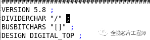
The student’s save method is as follows:
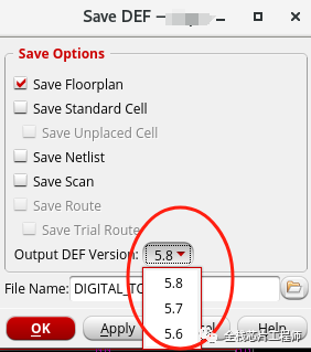
So how to solve it? Please join the Jingxin training camp for practice.
The Jingxin SoC uses many asynchronous FIFOs. Students interested in asynchronous RTL implementations can pull out the asynchronous FIFO to check the layout connections:
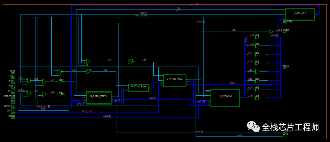
Check the area of all asynchronous FIFO cells;
dbget [dbget top.insts.pstatus unplaced -p].area
Check the names of all asynchronous FIFO cells:
dbget [dbget top.insts.pstatus unplaced -p].name
So how to extract the asynchronous path to observe the layout routing? How to report timing? For more content, please refer to the knowledge community and SoC training camp.
Frontend Design Directory
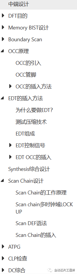
Mid-end Design Directory
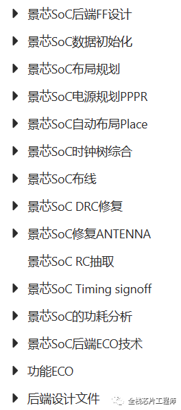
Backend Design Directory
Welcome to join the [Full Stack Chip Engineer] knowledge community to exchange technology, from algorithms, frontend, DFT to backend full-process design exchange.Click the image below to join the knowledge community!

Welcome to join the SoC MCU Full Process Design Exchange Group, first add my WeChat, verify the position, then join the group!
SoC MCU Full Process Design Exchange Group 4
SoC MCU Full Process Design Exchange Group 3
SoC MCU Full Process Design Exchange Group 2
SoC MCU Full Process Design Exchange Group 1
Welcome to join the CMOS Image Sensor + ISP Exchange Group, first add my WeChat, verify the position, then join the group!
CMOS Image Sensor + ISP Exchange Group 2
CMOS Image Sensor + ISP Exchange Group 1