
In the power-off module, it may be required for the register to latch the data before shutdown or to restore the latched data after the power is turned on, which requires a special unit called the Retention Register.
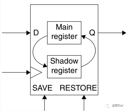
The retention register has two sets of registers: the Main Register and the shadow register, where the shadow register uses an always-on power supply;
It has two power sources, one for operational power when the module power is not off, and another for power when the module power is off. It also has two control signals: save and restore, used to control whether to latch data or restore data;
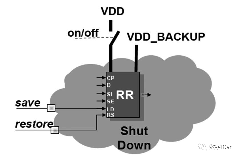
As shown in the figure above, this register requires two power sources: one is the always-on VDD_BACKUP for the shadow register, and the other is the switchable VDD for the Main Register.
When it is necessary to retain the state, enabling the SAVE signal will cause the value of the Main Register to be stored in the shadow register, and even if VDD is turned off, the value of the shadow register will still be retained. When the module/IP is powered on again, the value from the shadow register can be written back to the Main Register by enabling the RESTORE signal;
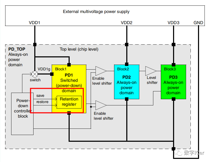
For power domains that can be turned off, such as PD1 in Block1 shown in the figure below, all internal data is lost after the power is turned off. If you want to keep this data after power loss, there are several methods:
-
Before power loss, store the internal data in external RAM and read the data back after power is restored; -
Use a Retention Register in power domains that can be turned off. Its internal structure is shown in the figure above; this register can save data from the Main Register to the internal Shadow Register through the SAVE signal before the power is turned off. After power is restored, the data can be restored from the Shadow Register to the Main Register through the RESTORE signal.
Like various low-power cells mentioned earlier, the Shadow Register inside the Retention Register is also an Always On Cell, which must have an always-on power supply. The Shadow Register is connected to the always-on power supply to ensure it operates normally. Because it is always on, to achieve low power goals, high-threshold MOSFETs are often used internally to reduce Leakage Power in Power Down mode.
In addition to the Shadow Register, other devices in the Retention Register use switchable power. For high performance and fast data recovery, the Main Register may also use low-threshold transistors.
Compared to conventional registers, the Retention Register occupies a larger area, typically about 20% larger than ordinary registers, and if the design robustness is good, it may even exceed 50%. However, compared to other solutions, the speed of data recovery after power-on is very fast, and the operation is also simple. Therefore, using a retention register requires special attention to the extra area and power consumption it brings. When too much data needs to be saved during power-off, the power consumption brought by the retention cell may discount the overall low-power effect.
QA1
In low-power design, the retention register actually contains two registers, one called the shadow register which uses always-on power for restoring register values. So why not use a normal register with always-on power directly? Wouldn’t that save one register?
Theoretically, a normal register could be used, but in practice, isolation must be considered. Just for clock, data, and reset, three isolation cells are needed. This results in higher power consumption, and it also affects timing.
The retention register internally takes these into account. As long as the signal entering the retention is always on, and the speed of entering and exiting the retention is very slow, it will not affect timing.
QA2
What do retention registers refer to? How are they different from general registers, and what are their main functions?
The retention register has two sets of registers, one of which is the shadow register using always-on power. Before power down, the value of the main register is loaded into the shadow register, and after power up, the value is loaded from the shadow register back to the main register. Since the shadow register is only used to store data, it can be made smaller, resulting in lower power consumption.
Using retention registers will increase additional leakage, so it needs to be used in conjunction with the system’s power-saving plan, and it will also increase additional area;
QA3
It seems that the retention registers have an additional shadow register, which seems to consume more power. How can it achieve power savings?
The key is that the shadow register in the retention registers only consumes a small amount of power to retain information, allowing the main register to completely power down, thus saving power;
QA4
What is the difference between the main and shadow registers in retention registers?
The main register has a larger area, operates at a higher voltage, and uses low-threshold voltage transistors, resulting in a large operating current. This ensures that the register is fast and has strong load capacity during normal operation.
The shadow register is relatively smaller, uses high-threshold voltage transistors, and its driving voltage is lower. Therefore, it consumes very little power.
Liberty Retention Register, For Reference Only
The lib description of retention registers specifies the power pins and input signals that control data saving and restoring.
It specifies which power pins are normal and can be powered down, and which are used to maintain data during power down.
cell(RETENTION_DFF) {
 retention_cell:"ret_dff";
 area : 1.0;
 ...
 pg_pin(VDDB) {
 voltage_name : VDDB;
 pg_type : backup_power;
 }
 ...
 pin(RETN) {
 direction : input;
 capacitance : 1.0;
 nextstate_type : data ;
 related_power_pin :VDDB;
 related_ground_pin:VSSG;
 retention_pin (save_restore, "1" );
 }
 pin(Q) {
 power_down_function:"!VDD+VSS";
 related_power_pin : VDD ;
 related_ground_pin : VSS;
 direction : output;
 ...
References
-
Synopsys® Low-Power Flow -
https://zhuanlan.zhihu.com/p/104415592 -
https://www.shangyexinzhi.com/article/589062.html