

Low Power Design Techniques: Power Gating and Isolation Cells
Previously, we discussed the Multi Vdd technology and Power Gating technology in low power design:
Low Power Design Techniques – Multi VDD
Low Power Design Techniques – Power/Ground Gating – Power Switching Cell
In the introduction of Power Gating, we detailed the Power Switching Cell; here we will discuss the Isolation Cell.
We know that in CMOS digital logic circuits, when a signal is at VDD, it is considered logic 1, and when it is at GND, it is logic 0. However, when a certain circuit is powered off, its output loses drive, and if the output network is not driven by other signals, its level will be in a high-impedance state. In other words, the voltage is unknown (it needs to rely on leakage current to slowly dissipate the charge).
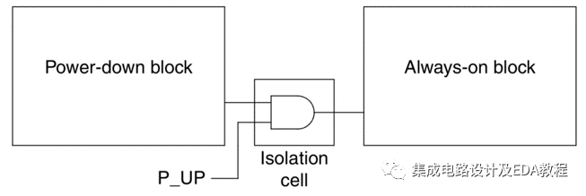
Therefore, in low power design, if it is necessary to cut off the power supply to a certain circuit, the output of that circuit will show an indeterminate value, and the circuits connected to these outputs will also enter a floating state. Thus, an Isolation Cell needs to be added between the output of the powered-off circuit and its connected modules. When the power is off, it fixes the output network at a certain level, and when the power is on, the output of that circuit equals the input, without affecting the circuit’s functionality.
The Isolation Cell can be implemented using logic gates; using an AND gate can make the output 0 when the power is off, known as a Low Clamped Isolated Signal, while using an OR gate can make the output 1 when the power is off, known as a High Clamped Isolated Signal. As shown in the figure below, X is the output signal, and “ISOLN” and “ISOL” are the switch control signals:
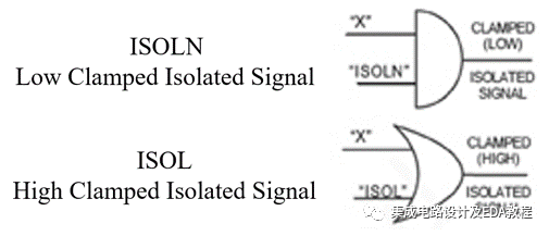
Isolation Cell Composed of Logic Gates
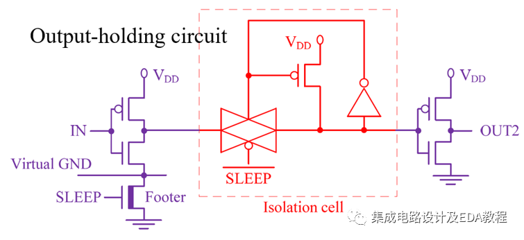
The Isolation Cell composed of logic gates will introduce delay, which may affect very fast circuits; therefore, a single N-MOS or P-MOS can be used to implement Pull-Up and Pull-Down circuits, but this can cause multiple driving issues and is not commonly used.
In addition, there is another type of output hold circuit, used to maintain the output during circuit shutdown, with the following structure:
The Isolation Cell composed of logic gates is a common cell. Below is a Liberty format description of an Isolation Cell:
|
cell(isolation_cell) { is_isolation_cell : true ; # Defines this Cell as an isolation_cell … pg_pin(<pg_pin_name_P>) { # Power Pin definition pg_type : primary_power; … } pg_pin(<pg_pin_name_G>) { # Ground Pin definition pg_type : primary_ground; … } pin (data) { direction : input; isolation_cell_data_pin : true ; # Controlled input Pin … }/* End pin group */ pin (enable) { isolation_cell_enable_pin : true ; # Control signal … }/* End pin group */ … pin (output) { # Output signal direction : output; power_down_function : (!pg_pin_name_P + pg_pin_name_G); # Enters power down state after power is off … }/* End pin group */ }/* End Cell group */ |
References:
Dr. Hailong Jiao, Low Power and Variations-Tolerant Digital IC Design in Nanoscale Regime
Sun Yiqun, Guomin Technology Co., Ltd., Low Power Physical Implementation Technology of Digital Integrated Circuits and UPF
H. Kim and Y. Shin, “Semicustom design methodology of power gated circuits for low leakage applications,” IEEE Transactions on Circuits and Systems II, Vol. 53, No. 10, pp. 1093-1097, October 2006.
Synopsys Low-Power Flow User Guide