Low Power Design Strategies for Operational Amplifiers

Introduction

In recent years, the popularity of battery-powered electronic products has made power consumption an increasingly important issue for analog circuit designers. This article will introduce how to use low-power operational amplifiers for system design, while also covering low-power operational amplifiers with low supply voltage capabilities and their applications. We will discuss how to correctly understand the specifications in the operational amplifier datasheets, comprehensively consider energy-saving technologies in circuit design, and achieve more efficient component selection.

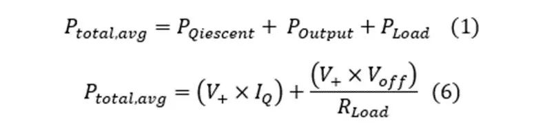
Understanding Power Consumption in Operational Amplifier Circuits

First, we will discuss amplifiers with low quiescent current (IQ) and the relationship between increasing the feedback network resistance and power consumption.
Let’s first consider an example circuit that may require attention to power: a battery-powered sensor generating a 50mV amplitude and 50mV offset analog sine wave signal at 1kHz. The signal needs to be amplified to a range of 0V to 3V for signal conditioning (Figure 1), while conserving battery power as much as possible. This will require a gain of 30V/V in a non-inverting amplifier configuration, as shown in Figure 2. So, how should we optimize the power consumption of this circuit?
Low Power Design Strategies for Operational Amplifiers
Figure 1: Input and output signals in the example circuit (Image source: Texas Instruments)
Low Power Design Strategies for Operational Amplifiers
Figure 2: Sensor amplification circuit (Image source: Texas Instruments)
The power consumption of operational amplifier circuits consists of various factors, including quiescent power, operational amplifier output power, and load power. Quiescent power (or simply PQuiescent) is the power required to keep the amplifier on, which is generally indicated by IQ (quiescent current) in the datasheet, as shown in the figure below from the Texas Instruments OPA391 datasheet.
Low Power Design Strategies for Operational Amplifiers
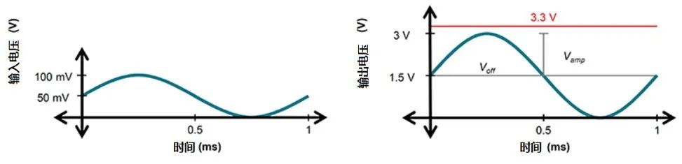
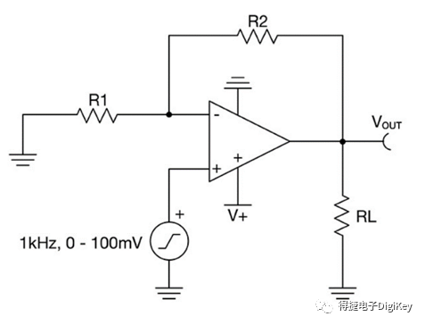
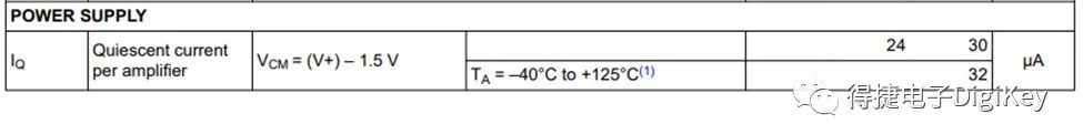
Figure 3: Quiescent current of TI OPA391 (Image source: Texas Instruments)
Output power (POutput ) is the power consumed by the operational amplifier output stage driving the load. Lastly, load power (PLoad) is the power consumed by the load itself.
In this example, we have a single-supply operational amplifier with a sine wave output signal having a DC voltage offset. Therefore, we will use the following equation to calculate the total average power (Ptotal avg). The supply voltage is represented by V+, Voff is the DC offset of the output signal, Vamp is the amplitude of the output signal, and RLoad is the total load resistance of the operational amplifier. It is important to note that the average total power is directly proportional to IQ and inversely proportional to RLoad.
Low Power Design Strategies for Operational Amplifiers

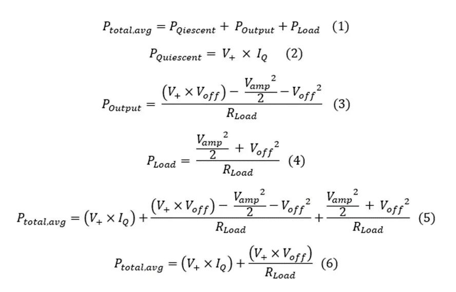
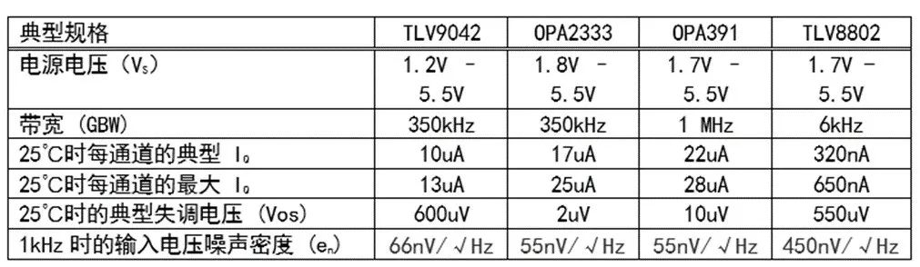
Choosing Components with AppropriateIQ Values

Since there are multiple variables in the equations above, it is best to consider only one variable when selecting components. Choosing amplifiers with low IQ is the most direct strategy to reduce overall power consumption. Of course, there are trade-offs in this process. For example, devices with lower IQ typically have lower bandwidth, higher noise, and may be more difficult to stabilize.
Since different types of operational amplifiers can have orders of magnitude differences in IQ, it is worth taking the time to select the appropriate amplifier. The following TI models: TLV9042, OPA2333, OPA391, and TLV8802 are compared. Based purely on numerical analysis, for applications requiring maximum power efficiency, TLV8802 would be a great choice.
Low Power Design Strategies for Operational Amplifiers
Table 1: Comparison of Various Low-Power Operational Amplifiers

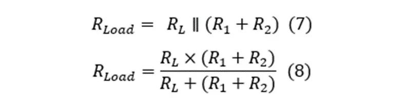
Reducing the Resistance Value of the Load Network
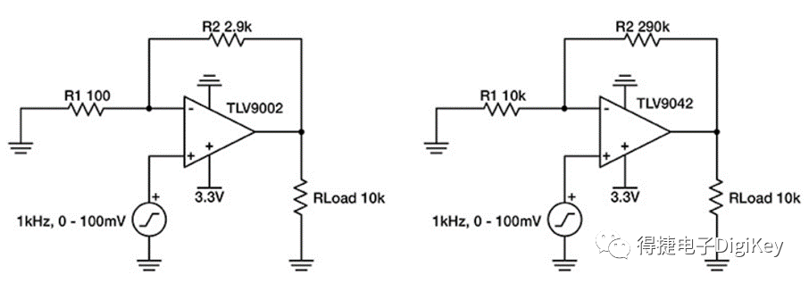
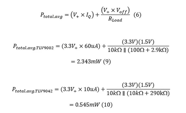
Now let’s continue considering the remaining terms in equations 5 and 6. The Vamp term cancels out and has no effect on Ptotal,avg and Voff, which are usually predetermined in the application. In other words, the system cannot use Voff to reduce power consumption. Similarly, the V+ rail voltage is typically set by the available supply voltage in the circuit. Additionally, RLoad is also predetermined by the application. However, RLoad includes any components that output load, not just the load resistor RL. In the case of the circuit shown in Figure 1, RLoad will include RL and the feedback components R1 and R2. Therefore, RLoad will be defined by equations 7 and 8 as follows.
Low Power Design Strategies for Operational Amplifiers
By increasing the value of the feedback resistor, the output power of the amplifier in the system is also correspondingly reduced. This technique is particularly effective when Poutput dominates PQuiescent, but it also has its limitations. If the feedback resistor becomes significantly larger than RL, then RL will dominate RLoad, causing power consumption to stop decreasing. Large feedback resistors can also interact with the input capacitance of the amplifier, making the circuit unstable and generating significant noise.
To minimize the noise generated by these components, it is best to compare the thermal noise of the equivalent resistance seen at each operational amplifier input (see Figure 4 below) with the voltage noise spectral density of the amplifier. A rule of thumb is to ensure that the input voltage noise density specifications of the amplifier are at least three times greater than the voltage noise generated by the equivalent resistance observed from each input of the amplifier.
Low Power Design Strategies for Operational Amplifiers
Figure 4: Thermal noise of resistors (Image source: Texas Instruments)

Real-World Examples

Using these low-power design techniques, let’s return to the initial question: a battery-powered sensor generating a 0 to 100mV analog signal at 1kHz requires a 30V/V signal gain. Figure 5 compares two designs. The design on the left uses a typical 3.3V power supply, resistors that do not consider energy saving, and the TLV9002 general-purpose operational amplifier. The design on the right uses larger resistor values and the lower power TLV9042 operational amplifier. Note that when the equivalent resistance at the inverting input of the TLV9042 is approximately 9.667kΩ, the noise spectral density is less than one-third of the amplifier’s broadband noise to ensure that the noise generated by the resistor dominates over the amplifier’s noise.
Low Power Design Strategies for Operational Amplifiers
Figure 5: Typical design vs. refined design (Image source: Texas Instruments)
Using the values, design specifications, and the datasheets of the two operational amplifiers in Figure 5, we can apply equation 6 to derive Ptotal,avg for both the TLV9002 design and the TLV9042 design. The results are shown in equations 9 and 10 respectively.
Low Power Design Strategies for Operational Amplifiers
From the above results, it can be seen that the power consumption of the TLV9002 design is more than four times that of the TLV9042 design. This is the result of the higher IQ of the amplifier, which also shows that utilizing operational amplifiers with high IQ, even when attempting to use low feedback resistor values, will not yield significant power savings. In the above example, we have two strategies, which are increasing resistor values and selecting operational amplifiers with lower quiescent currents. Both strategies are applicable in most operational amplifier applications.

Saving Power with Low Voltage Rails

Let’s revisit equations 1 and 6, which define the average power consumption of a single-supply operational amplifier circuit with a sine wave signal and DC offset voltage:
Low Power Design Strategies for Operational Amplifiers
Additionally, the V+ in equation 6 represents the power rail voltage (V+), which is directly proportional to power consumption, so setting the power rail (V+) to the lowest available supply voltage in the circuit is another method for reducing power consumption. Many operational amplifiers have a minimum supply voltage range of 2.7V or 3.3V. This limitation is due to the minimum voltage needed to keep the internal transistors within the desired operating range. Some operational amplifiers are designed to work at voltages as low as 1.8V or even lower. For example, the TLV9042 general-purpose operational amplifier can operate at a voltage rail of 1.2V.

Battery-Powered Applications

Today, most sensors and smart devices are battery-powered, and the terminal voltage of the battery decreases as it discharges. For example, a standard alkaline AA battery has a nominal voltage of 1.5V. The actual terminal voltage may be close to 1.6V when measured under no load. As the battery discharges, the terminal voltage may drop to 1.2V or even lower.
Using operational amplifiers that can work at voltages as low as 1.2V instead of higher voltage operational amplifiers can provide the following advantages:
1. Operational amplifier circuits will continue to work longer, even when the battery is nearing the end of its charge cycle and its terminal voltage drops.
2. Operational amplifier circuits can operate with a single 1.5V battery without needing two batteries to form a 3V power rail.
To understand why operational amplifiers with lower operating voltages can achieve longer battery life, consider the battery discharge curve shown in Figure 6. Batteries typically have a discharge cycle similar to this curve. The terminal voltage of the battery will start close to its nominal rated value. As the battery discharges over time, the terminal voltage gradually decreases. Once the battery approaches the end of its charge, the terminal voltage drops rapidly. If the operational amplifier circuit is designed to operate only at voltages close to the battery’s nominal voltage, such as V1, then the circuit’s operating time t1 will be very short. However, using operational amplifiers that can work at slightly lower voltages, such as V2, can significantly extend the battery’s operating life t2.
Low Power Design Strategies for Operational Amplifiers
Figure 6: Typical discharge curve of a single battery (Image source: Texas Instruments)
While this effect may vary depending on battery type, load, and other factors, it is clear that operational amplifiers with low operating voltages can achieve longer operating times.

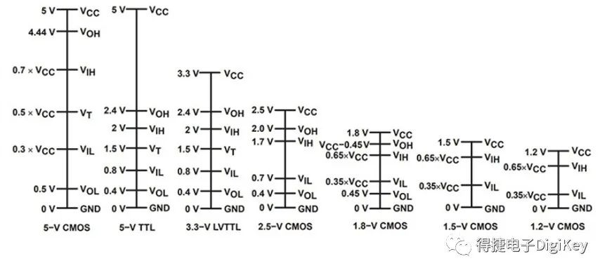
Low Voltage Digital Logic Levels

Applications using low voltage rails for both digital and analog circuits can also benefit from low-power operational amplifiers with low supply voltage capabilities. Digital logic has standard voltage levels ranging from 5V to 1.8V and below (Figure 7). Similar to operational amplifier circuits, digital logic becomes more energy-efficient at lower voltages. Therefore, lower digital logic levels are often preferred.
To simplify the design process, you can choose to use the same supply voltage levels for your analog and digital circuits. In this case, operational amplifiers with 1.8V capability (such as high-precision, wide-bandwidth OPA391 or cost-optimized TLV9001) can prove advantageous. However, it is important to ensure that if the design is to be applicable to a 1.2V digital rail, the line system must clear any noise that may leak from the digital circuit to the analog device power pins.
Low Power Design Strategies for Operational Amplifiers
Figure 7: Standard logic levels (Image source: Texas Instruments)

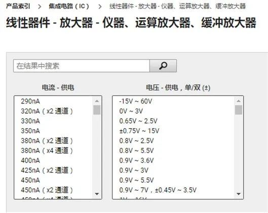
Digi-Key Operational Amplifier Parameter Filtering Tool

When engineers are designing low-power operational amplifiers for systems, the parameter filtering tool on the Digi-Key website can assist engineers in component selection, such as: “Current – Power Supply,” which allows engineers to understand the current required by the operational amplifier; “Voltage – Power Supply, Single/Dual (±),” which describes the low supply rail requirements mentioned in the article. Here, engineers can clearly understand the supply rail, making it easier to complete the selection process quickly.
Low Power Design Strategies for Operational Amplifiers
Figure 8: Digi-Key operational amplifier parameter filtering tool

Conclusion

In this article, we introduced how to quickly identify operational amplifiers that provide low power characteristics using the parameter specifications of operational amplifiers. These methods include selecting low quiescent current operational amplifiers within the bandwidth allowance and choosing larger resistor values in the feedback circuit. Choosing to use low voltage rails and low voltage digital logic levels are also two additional factors to consider for ensuring low power in operational amplifiers.
Source: Digi-Key Electronics
Low Power Design Strategies for Operational Amplifiers

Low Power Design Strategies for Operational Amplifiers

Low Power Design Strategies for Operational Amplifiers
Click to read the original text and register for the event

Leave a Comment