Cassie Ren, an architecture expert at Fuzhuo Microelectronics, graduated from the National University of Singapore and has extensive experience in low power chip design and information security, having previously worked at Realtek Semiconductor in Singapore.
From the relevant policies being introduced, it is clear that the autonomous driving industry is a key area currently supported by the government. In recent years, China’s autonomous driving industry has flourished with multi-faceted support. As software and hardware conditions mature, new cars equipped with L2-level autonomous driving functions are gradually becoming standard for smart vehicles. Currently, the level of autonomous driving in mass-produced passenger vehicles in China is transitioning from L2 to L3+, and many tech companies have begun developing L4-level autonomous driving chips and solutions. With the increasing market demand for higher levels of autonomous driving, the computational power requirements for the chips used in vehicles are also rising, which in turn leads to higher power consumption. For consumers and car manufacturers, the issue of power consumption has always been a focal point. How to achieve low power consumption with high performance is a challenge that chip designers and their upstream partners must address together.
Advantages of Reducing Power Consumption
Why is power management necessary? Let’s discuss briefly.
1) Excessive power consumption shortens usage time. As users of electronic devices like smartphones know, frequent charging greatly reduces user experience.
2) Excessive power consumption can lead to higher temperatures, which may cause electronic migration or other thermal failure mechanisms, thereby reducing chip stability.
3) For vehicles, if the power consumption of autonomous driving chips exceeds a certain limit, manufacturers will need to adopt water cooling measures instead of air cooling systems, which will also increase the overall manufacturing costs.
4) High power consumption can also affect battery life, resulting in shorter battery lifespans, which increases consumer costs and reduces product experience.
Therefore, the power consumption of the system-on-chip (SoC) is a very important topic. As chip designers, ensuring that the autonomous driving chips used in smart vehicles have lower power consumption is a continuous focus throughout our work, from the early selection of non-self-developed IP for chips, to mid-stage chip design, to later software and solutions. We strive to reduce chip power consumption at every stage while providing more stable and competitive autonomous driving chips in terms of computational power.
Methods to Reduce Power Consumption[1]
First, two concepts need to be introduced: dynamic power and static power. The power consumption of an SoC includes dynamic power (Dynamic Power) and static power (Static Power).
Dynamic power is the power loss due to changes in signal values. Dynamic power consists of two parts: switching power and internal power. Switching power is the power consumed during the charging and discharging of external capacitance (as shown in Figure 1), while internal power is the power consumed by the short-circuit current flowing through the PMOS-NMOS stack when the circuit logic state changes (as shown in Figure 2).
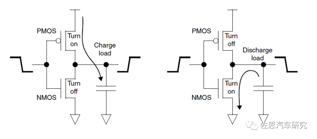
Figure 1
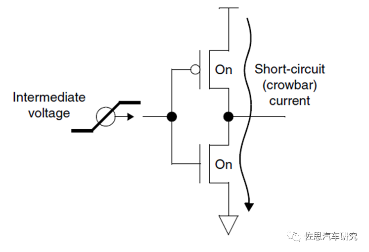
Figure 2
Static power is the power consumed when the device is powered on but there are no changes in signal values. In CMOS devices, static power originates from leakage current (as shown in Figure 3).
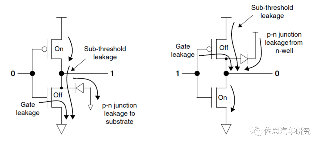
Figure 3
Ways to Reduce Power Consumption
2.2.1 Supply Voltage Reduction
The most fundamental way to reduce power consumption is to lower the supply voltage. Power consumption is proportional to the square of the voltage. Therefore, if the voltage is reduced by 50%, power consumption will decrease by 75% (as shown in Figure 4). The continuous evolution of CMOS technology has led to lower supply voltages to reduce power consumption, with supply voltages dropping from 5V in the 1980s to current levels of 0.75V or even lower.
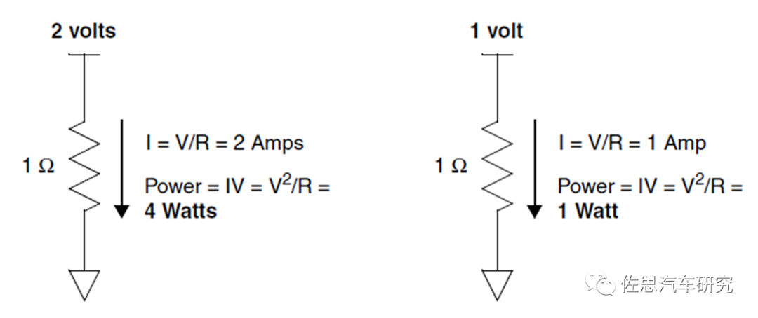
Figure 4
2.2.2 Clock Gating
Clock gating is a method to reduce dynamic power consumption. For registers that need to maintain the same value for many clock cycles, this method is particularly useful, as it avoids unnecessary power loss from reloading the register in each clock cycle. The biggest challenge of this method is finding the optimal locations to place clock gating to ensure that clocks are switched on and off at appropriate times.
Clock gating technology has been in use for many years and is quite mature. Tools like Power Compiler can detect low-throughput data paths and automatically insert clock gating units at appropriate locations in the clock path. The implementation of clock gating is also relatively simple; it only requires modifying the netlist without the need to add extra power supplies or other power facilities.
2.2.3 Multiple-Vt Library Cells
Some CMOS technologies support standard library cells with different voltage thresholds. In this case, the cell library can provide two or more different threshold voltage cells to achieve the same logic function. For example, the library can provide two types of inverter cells: one with low-Vt transistors and one with high-Vt transistors.
Low-Vt cells have higher speed but also higher leakage current. High-Vt cells have lower leakage current but slower speed. Therefore, synthesis tools can select the appropriate type of cell based on the trade-off between speed and power consumption. For instance, low-Vt cells can be used in timing-critical paths for higher speed, while high-Vt cells can be selected for paths where timing requirements are less stringent to reduce power consumption.
2.2.4 Multi-voltage Design
Different parts of a chip have different speed requirements. For instance, CPUs and RAM require higher speeds than peripherals. As mentioned earlier, lower voltage not only reduces power consumption but also reduces speed. To achieve maximum speed with lower power consumption, higher supply voltages can be provided to the CPU and RAM, while lower supply voltages can be given to peripheral components. However, providing two or more supply voltages on the same chip increases design complexity and cost, as more pins are needed to supply power to the chip, and the power grid must separately allocate each voltage source to the appropriate module.
2.2.5 Power Switching
Power switching is a method to save power by turning off the power to a chip module that is not used for a long time. For example, in a mobile phone chip, the sound processing module can be turned off when the phone is in standby mode. When a user receives or makes a call, this module will be awakened.
Power switching further reduces both static and dynamic power consumption. However, it also brings some challenges, such as the need for a power controller, a power switch network, isolation cells, and retention registers.
The power controller is a logic module that decides when to turn the power on and off. However, turning power on and off incurs a certain time and power cost, so the controller must determine an appropriate time to switch the power.
A module that can be powered down must receive power from the power switching network, which consists of many transistors connected from always-on power rails to power pins. The power switch must be placed around or within that module. When the power is turned on, it connects the power to the logic gate, and when the power is turned off, the power supply is disconnected from the logic gate.
We often use high-Vt transistors as power switches because they have lower leakage current, and we do not care about their switching speed. As shown in Figure 5, a PMOS header switch can be placed between VDD and the module power supply pin, or an NMOS footer switch can be placed between VSS and the module ground pin.
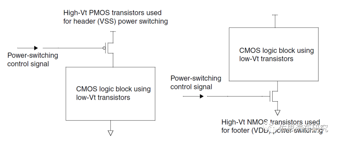
Figure 5
The power switching strategy described above is a coarse-grained switching strategy, as this power switch can control the power on and off for the entire module. In contrast, a fine-grained strategy would allow each library cell to have its own power switch, allowing for more granular control of power on and off. This method can save more power but also requires more area.
2.2.6 Dynamic Voltage Frequency Scaling
Based on the previously mentioned multi-voltage concept, we can extend it to dynamically adjust voltage during operation based on the current workload. For example, a chip performing simple calculations can use lower voltage and frequency, while higher voltage and frequency can be used when higher performance is required. This real-time adjustment of voltage and frequency is called DVFS.
The chip’s supply voltage can be designed with multiple levels or a continuous range, and dynamic voltage adjustment requires multi-level power supplies and a logic module capable of accurately determining the optimal voltage value for a given task. This presents considerable challenges for design, execution, verification, and testing due to the need to analyze and consider combinations of different voltage levels and frequencies.
We can combine dynamic voltage adjustment with power switching, allowing modules to adjust voltage based on current workload while also turning off power when not in use, achieving greater power savings.
Power Management Module[2]
With the increasing complexity of modern SoCs, more and more chip designers are opting to separate the role of power management within the SoC, choosing a small processor combined with software to manage the power consumption of the entire SoC.
Previously, operating systems (OS) managed the power and performance of SoCs, but it has become increasingly difficult to create and maintain a universal OS kernel that supports different vendors. Moreover, modern SoCs have more and more restrictions, forcing them to meet stringent functional safety and information security requirements, which are too complex for an OS to manage while ensuring optimal load performance. This has led the industry to separate the OS-based centralized control mechanism, creating a dedicated small system to control and manage power consumption and performance.
As mentioned earlier, dynamic voltage frequency scaling (DVFS) selects {frequency, voltage} pairs based on the OS workload, which requires the OS kernel to be aware of all the {frequency, voltage} pairs supported by the platform and how to read and set them. Each SoC has a different method for reading and setting information pairs, so if the OS kernel is to manage power consumption and performance, it needs to be modified according to the design of each SoC, which contradicts the desire to maintain the universality of the kernel. Therefore, we can record the supported {frequency, voltage} pairs in the power management small system and correspond performance levels with frequency-voltage pairs. The OS kernel only needs to issue requests to adjust frequency and voltage to the small system, which can then adjust them accordingly. This approach achieves control while maintaining the universality of the OS kernel.
In terms of functional safety, when an incidental event occurs, generally speaking, the response time of hardware is less than that of firmware, which is less than that of the kernel. Figure 6 shows the response times of hardware, firmware, and OS kernel to incidental events on the SoC platform in typical scenarios. As seen in Figure 6, the response time of the kernel is significantly longer than that of firmware. Moreover, the kernel cannot be aware of all the functional safety-related operations on the SoC, so these tasks can also be delegated to the power control small system. This small system has a faster response time and can guarantee functional safety while also having control over other hardware within the SoC.

Figure 6
Additionally, in terms of information security, the OS’s DVFS implementation is in the kernel, which is located in BL1, an untrusted area. It is risky for the kernel to have control over frequency and voltage. Untrusted software could put the SoC platform in an overclocked or undervolted state. Therefore, we transfer control over frequency and voltage to a trusted firmware, which can perform credibility checks on the required performance levels to prevent the dangers posed by malicious programming.
System Low Power Modes and Design
ACPI[3] defines four power states from G0 to G3, where G0 is the working state and G3 is the power-off state. G1 and G2 are further divided into sleep states S0ix to S5, defining the states of CPU, GPU, and memory modules in each sleep state (as shown in Table 1).
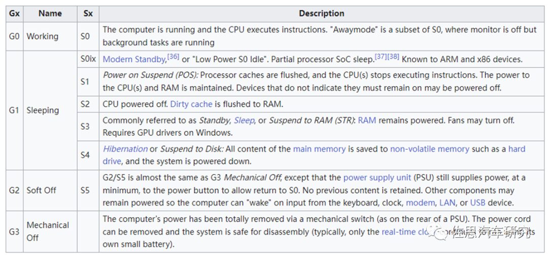
Table 1
For an SoC, it is essential to support both working and power-off states. However, the sleep state between these two states is determined by application requirements. The automotive industry is still in a developmental stage, and the power mode definitions for autonomous driving chips have not yet formed a fixed solution. Analyzing the current applications of autonomous driving chips in cockpit scenarios, many cars support a pre-installed sentinel mode, which requires that when the car is turned off and the person leaves the vehicle, the sensors on the car can detect nearby objects to awaken the cameras on the vehicle. Awakening the cameras means that the controlling chip must also be awakened to record and save the surrounding conditions through the camera. However, if the autonomous driving chip is completely powered down during this function, the time taken for the chip to power on and become operational might exceed 10 seconds, which does not meet the scenario requirements. Therefore, this necessitates that the autonomous driving chip supports a quick wake-up low power state in this mode. Why is a low power state needed? Because if it remains in the previous working state, the chip’s power consumption will be quite high, leading to rapid battery drain, which severely affects user experience and battery lifespan. Therefore, the pre-installed sentinel mode requires that the autonomous driving chip must support at least one low power mode.
Furthermore, some manufacturers may choose not to completely power down the autonomous driving chip and cockpit chip after the car is turned off, but rather keep them in an ultra-low power mode. The benefit of this approach is that once the ignition is turned on, the vehicle’s system can quickly return to the state it was in before leaving the vehicle. Generally, cockpit chips will use the Android system, which may take over ten seconds to boot, meaning that from the moment the car is started to when the display shows information may take several seconds or even longer, significantly reducing user product experience. The low power mode can save the software state in the DRAM connected to the LPDDR and keep the DRAM in a retention state, allowing only a small power processor subsystem to remain operational. This small processor can quickly restore the state to the vehicle’s system upon receiving a wake-up signal. This state consumes very little power and can wake up quickly, addressing the poor experience caused by slow operating system startup while consuming minimal energy. This function also requires that the autonomous driving chip supports low power modes.
Design of System Low Power Modes
4.1.1 Power Domains
First, we need to introduce the concept of power domains, which refer to collections of modules that share the same power switch logic within the same voltage domain. As mentioned earlier, multi-voltage design is a method to reduce power consumption, and different voltages correspond to different power domains. For modern SoCs with complex functionality, multi-power domain design is a necessary choice.
4.1.2 Low Power Mode Design Based on Multi-Power Domains
As mentioned earlier regarding the application scenarios of autonomous driving chips, how to support low power modes? The overall idea is to power down modules that are not needed in this mode to save dynamic and static power. For modules that cannot be powered down, we retain their power supply but choose their low power modes to achieve maximum power savings. For example, for memory, we need to retain the software stack information connected to LPDDR, and RAM characteristics dictate that data disappears once powered down, so we will adopt a power-saving mode that retains data without losing it – the Retention mode. Previously, we mentioned that the SoC’s power management module is a small system centered around a processor, so in this scenario, this processor needs to remain operational to monitor external wake-up signals and assist other processor cores in quickly restoring the state. We previously discussed power domains, and typically there will be an always-on power domain, which has the highest power level and the lowest priority for power down among all power domains. In low power mode, this processor must be powered on, so it is in the Always On power domain. The processor needs to operate, so the SRAM it uses must also be powered. Additionally, there must be GPIO to receive wake-up interrupt signals, which the GPIO will send to the processor. Upon receiving the wake-up interrupt, the processor will initiate its state restoration program. Therefore, in summary, the low power mode requires a power management subsystem to remain operational and the DRAM to be in Retention mode, which should include a processor core, a memory for running programs, GPIO for receiving wake-up signals, an interface for communication with PMIC, and an internal bus for connecting various submodules. This design of a power management small system combined with the retention state of DRAM can meet the need for quickly waking up the entire SoC while consuming very little power. The schematic diagram is shown in Figure 7, where the bright yellow represents the power management small system, which is in the Always-On power domain. In addition, a power supply is provided to the DDR PHY to maintain the DRAM’s Retention state.
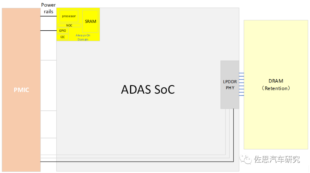
Figure 7
This article provides a brief introduction to power management for autonomous driving chips. In addition to the methods mentioned above, there are many other ways to save power. The chip is only a part of the industry chain; the overall system’s power control is the ultimate goal that requires the efforts of everyone involved.
[1] Synopsys® Low-Power Flow User Guide Version B-2008.09, September 2008
[2] Power and Performance Management using Arm® SCMI Specification
[3] https://en.wikipedia.org/wiki/ACPI
About Fuzhuo Microelectronics
Fuzhuo Microelectronics is an advanced technology company incubated by the Fortune Global 500 company Fosun Group. Rooted in an innovation-driven culture with a mission to enhance customer experience, the company is committed to “shaping the future of intelligent travel through innovative high-performance chip design,” focusing on the research and development and sales of high-performance chips and overall solutions in automotive electronics, artificial intelligence, and other fields. Currently, the company mainly engages in the research and development of automotive autonomous driving and intelligent cockpit chips, leading the new era of automotive intelligence through superior chip design capabilities and AI algorithm development, promoting innovation in the automotive industry and enhancing people’s travel experiences.
Article Reprint: Please indicate the source at the beginning of the article
Bus Consistency: Core Technology of High-Performance SoCs
4D Millimeter-Wave Radar on the Eve of Revolution
Societal Autonomous Driving Restructuring Computational Models
Chiplet: Wings of High Performance
Limitations of Machine Vision Algorithms
Reusability of NPU Data Streams in ADS Chips
Technical Evolution and Challenges of ADS Algorithms
A Brief Discussion on the Rapid Iteration and Evolution of Algorithms and Computational Power in the Autonomous Driving Industry