As IC engineers, you must have seen the requirement for low power design experience in job descriptions. What is low power design? For backend engineers, it involves introducing multiple power lines and providing power to different power domains based on the various voltage domains and the global power network designed according to the settings. To address potential issues that may arise during the power supply process for multiple power and voltage domains, low power cells need to be introduced. For simple voltage domain designs, engineers can manually global connect and then detail route without needing to consider the placement of low power cells or the setup of islands. However, for complex power networks, engineers need to introduce Power Intent files such as CPF (Common Power Format) and UPF (Unified Power Format) to implement complex multi-voltage domain designs, voltage domain shutdowns, and even dynamic voltage scaling (DVFS) to control voltage variations across different voltage domains.
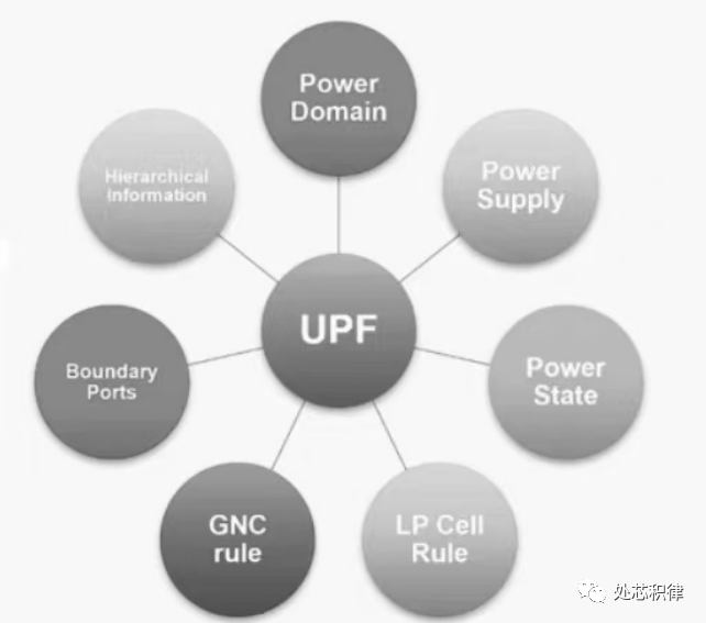 Figure 1 UPF files include/define the content of low power design
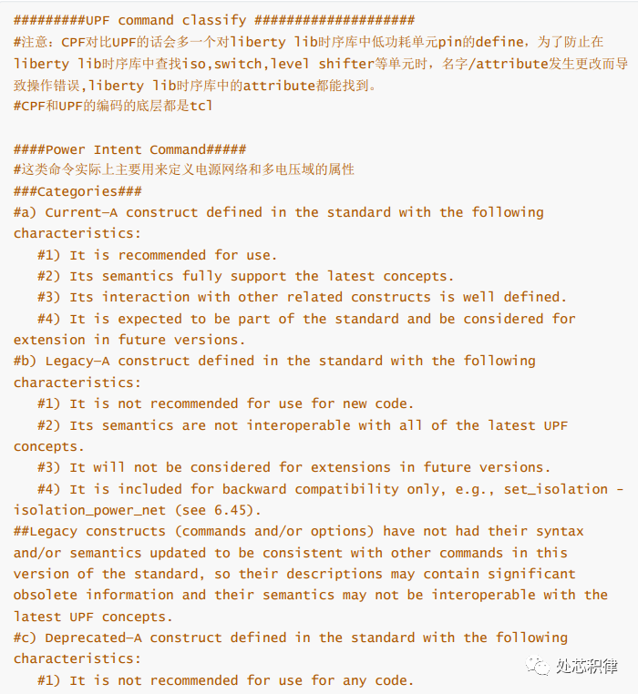
In fact, UPF focuses on describing and defining the chip’s power consumption architecture (such as the definition of voltage sources, power state definitions, connections between low power cells like ISO, MTCMOS (PSW), LVL, and ELS cells, power supply relationships, and layout information). The UPF file, like the SDC file, has its own writing style. UPF has long been recognized as a standard protocol. Backend engineers who have worked on low power designs should know that when importing UPF 3.0 into Innovus, the file is not called UPF but IEEE1801. The following diagram shows the UPF usage standards, which can be seen as the IEEE low power design standards, including the man page for UPF commands and usage notes.
UPF Coding Basics (Content: Power Network Definitions, Multi-Voltage Domain Designs, Low Power Modes, Low Power Cell Rules, Chip Edge Power Definitions, IP Power Descriptions)
Figure 1 UPF files include/define the content of low power design
In fact, UPF focuses on describing and defining the chip’s power consumption architecture (such as the definition of voltage sources, power state definitions, connections between low power cells like ISO, MTCMOS (PSW), LVL, and ELS cells, power supply relationships, and layout information). The UPF file, like the SDC file, has its own writing style. UPF has long been recognized as a standard protocol. Backend engineers who have worked on low power designs should know that when importing UPF 3.0 into Innovus, the file is not called UPF but IEEE1801. The following diagram shows the UPF usage standards, which can be seen as the IEEE low power design standards, including the man page for UPF commands and usage notes.
UPF Coding Basics (Content: Power Network Definitions, Multi-Voltage Domain Designs, Low Power Modes, Low Power Cell Rules, Chip Edge Power Definitions, IP Power Descriptions)
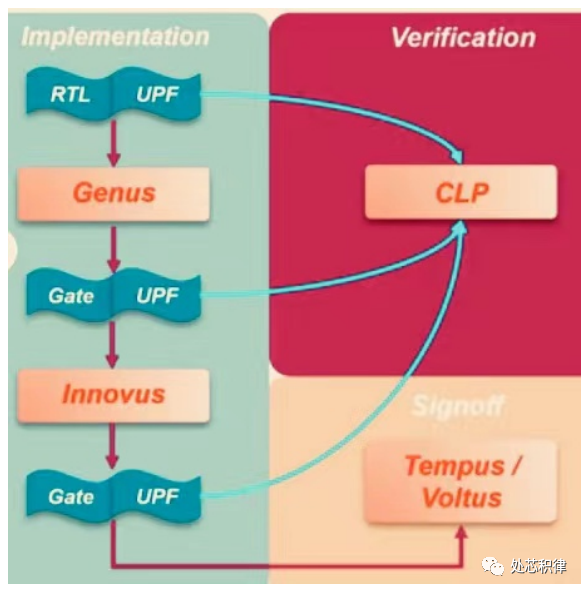
In fact, UPF runs through the entire backend design. Different voltage domains use corresponding library cells (including various .lib library collections), for example, 1.0V uses a 1.0V library, and 2.0V uses a 2.0V library. In synthesis, ISO, ICG, and LEVEL SHIFTER are generally added, while SWITCH cells (MTCMOS four-pin chains) are added in physical design. It is also worth noting that low power cells are generally added at the boundary of the power domain, but if some low power cells (ISO, level shifter) are added on the macro’s pins, they cannot be placed at the voltage domain boundary. CLP verification mainly checks whether the UPF architecture (the contents) is written correctly, implemented through Cadence’s conformal tool, while Tempus and Voltus are Cadence’s sign-off tools for PT and PI.
Figure 2 UPF Backend Full Process and Sign-off CLP, PI Verification Process
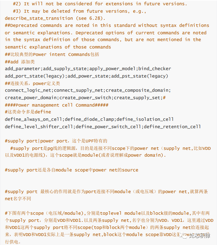
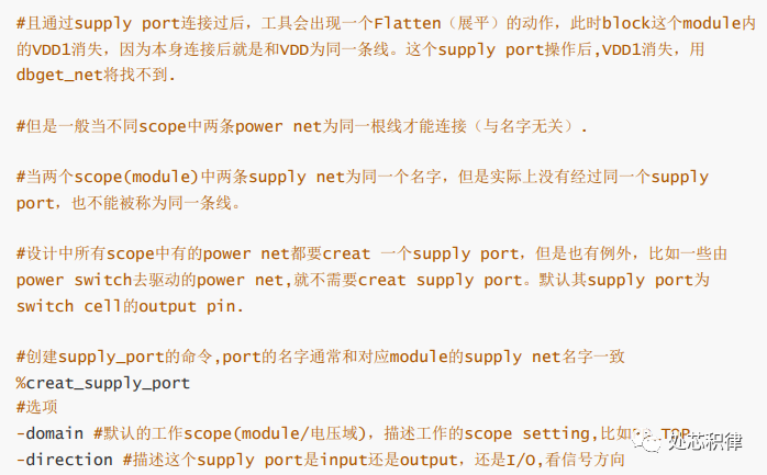
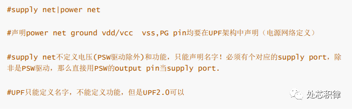
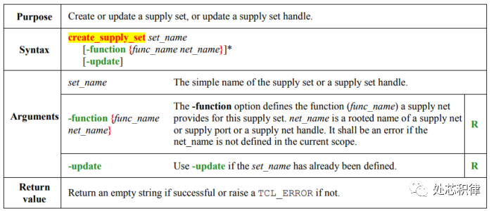
UPF Power Network Definition Supply Net
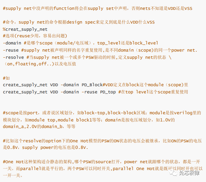
UPF Power Network Definition Supply Set
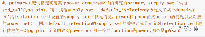
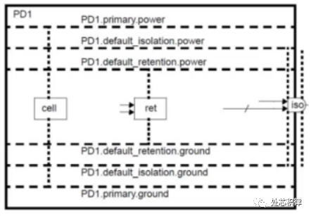
The figure shows that PD1’s supply set includes primary power for powering internal elements and a constant power grid net for ISO and retention.
At this point, I have introduced the general content of UPF coding and its application process in the backend, as well as the two important UPF create commands: supply_net and supply_set. Next time, I will take a multi-PD module’s UPF as an example to explain in detail and step by step the writing rules of UPF, making it easier for IC engineers to write low power UPF files, allowing everyone to plan power networks and voltage domain supplies for their project modules using UPF.
Originally published on Chuxin Jilv, thank you for reading!