The chip tape out (Tape Out) technology is a core part of semiconductor manufacturing, accurately transferring design patterns onto silicon wafers, serving as a critical bridge between design and production. This article comprehensively discusses chip tape out technology, from design, tape out preparation to technical implementation, equipment, and material applications, analyzing the key stages and challenges in the tape out process.
| StageDetails | Detailed Explanation |
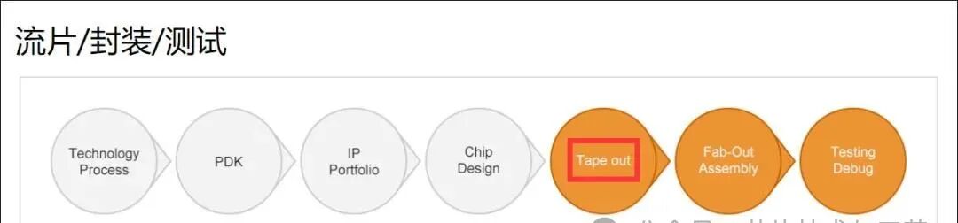
| Technology Process(技术工艺) | Selecting and defining the process technology required for chip manufacturing. Process technology includes the size of transistors, material selection, and detailed specifications of the manufacturing process. Different process technologies are suitable for different types of chips, such as high-performance processors and low-power devices. |
| PDK(Process Design Kit,工艺设计套件) | A set of tools and documents provided to chip designers, containing detailed information about process technology, design rules, and verification methods. Designers use PDK to ensure their designs meet the requirements of the manufacturing process, ensuring that the chips can be manufactured correctly. |
| IP Portfolio(知识产权库) | Includes pre-designed and verified functional modules (such as processor cores, memory modules, interface circuits, etc.). Designers can use these modules to accelerate the chip design process and reduce risks and errors in the design. |
| Chip Design(芯片设计) | Detailed design of the chip based on requirements and specifications in the PDK. The design includes logic design, physical design, and circuit layout. After the design is completed, simulation and verification are required to ensure that the chip’s functionality and performance meet the requirements. |
| Tape Out(流片) | Submitting the final design’s chip layout data to the manufacturer for production. This is an important milestone in the chip manufacturing process, marking the end of the design phase and the beginning of the manufacturing phase. |
| Fab-Out Assembly(晶圆制造和封装) | Includes wafer manufacturing and chip packaging. The wafer manufacturing process involves a series of complex steps, such as photolithography, etching, ion implantation, etc. After manufacturing, the wafer is cut into individual chips and then packaged to protect the chip and provide electrical connections. |
| Testing Debug(测试和调试) | After manufacturing and packaging, the chip enters the testing and debugging phase. Testing includes functional testing, performance testing, and reliability testing to ensure that the chip works properly under various conditions. If problems are found, debugging and repairs are necessary. |
#01Introduction
1.1 Definition of Chip Tape Out
Chip tape out is a key part of semiconductor manufacturing, referring to the process of converting the designed chip pattern from computer data into a physical structure on actual silicon wafers. This process includes precision techniques such as photolithography, etching, ion implantation, and metal deposition, ensuring the accurate construction of integrated circuits on the silicon wafer according to the design.

*Focused Ion Beam (FIB) technology is a technique that uses high-energy ion beams for micro-processing and analysis.
| Item | Detailed Explanation |
| Technical Principle | Focused ion beam technology uses high-energy ion beams (usually Ga+ ions) focused on the sample surface, performing nano-level processing and analysis through the physical impact and sputtering of ions on the sample. |
| Main Components | 1. Ion Source: Generates high-energy ion beams, commonly using liquid metal ion sources (LMIS). 2. Focusing System: Uses electric and magnetic fields to focus the ion beam onto the sample surface. 3. Sample Stage: Used to fix and move the sample, enabling processing and analysis of specific areas. |
| Application Fields | 1. Semiconductor Manufacturing: Used for circuit repair, fault analysis, and cross-section preparation. 2. Materials Science: Used for nano-level processing, surface modification of materials, and cross-section analysis. 3. Life Sciences: Used for fine processing and analysis of biological samples. |
| Main Functions | 1. Nano Processing: By precisely controlling the ion beam, nano-level engraving and cutting can be performed on the sample surface. 2. Cross-section Preparation: Used to create fine cross-sections of samples for subsequent microscopic analysis. 3. Element Analysis: Combined with energy-dispersive X-ray spectroscopy (EDX), element composition analysis can be performed. |
| Advantages | 1. High Precision: Capable of nano-level processing and analysis. 2. Multifunctional: Integrates processing, analysis, and imaging functions. 3. Non-contact: The ion beam does not directly contact the sample, avoiding mechanical damage. |
| Limitations | 1. Damage Effects: High-energy ion beams may cause damage and contamination to the sample. 2. Material Selection: Some materials may not respond well to ion beams, potentially affecting processing results. 3. High Cost: Equipment and operational costs are relatively high. |
| Recent Advances | In recent years, focused ion beam technology has made significant progress in high-resolution processing and non-destructive analysis. Improvements in new ion source materials and focusing systems have expanded the application range of FIB, especially in nanotechnology and biomedical fields. |
With the advancement of semiconductor technology, the chip tape out process continues to innovate. For example, micro end mill technology simplifies the manufacturing process of microchannel chips, reducing production costs. The success of chip tape out relies on multi-faceted technical collaboration, such as the partnership between SMIC and Zhaoxin Semiconductor to achieve the tape out of a 40nm low leakage ARM Cortex-A9 dual-core test chip, demonstrating the close cooperation between design, manufacturing, and testing stages.
The importance of chip tape out technology in semiconductor manufacturing cannot be overlooked. It is not only a key step in transforming chip design into actual products but also a core driving force for technological innovation and industrial development in the semiconductor industry. With technological advancements and growing market demand, chip tape out technology will continue to play an indispensable role.
1.2 Importance of Chip Tape Out
Chip tape out occupies an important position in semiconductor manufacturing, serving as a critical step in transforming chip design into actual products and as a bridge connecting design and production. Here are several aspects of its importance:
- Realizing Chip Design Implementation: The tape out process transfers the designed chip pattern through a series of precise manufacturing steps onto the silicon wafer, forming integrated circuits with specific functions. The success of tape out means that the designed chip can be smoothly transformed into a tangible product in the market, directly affecting the chip product’s emergence and market competitiveness.
- Process Optimization and Cost Control: Process optimization and cost control during the tape out process are crucial for the market competitiveness of chips. With the development of semiconductor technology, the complexity and cost of chip manufacturing are also rising. Through process optimization, production costs can be reduced, and production efficiency can be improved, making chip products more competitive in the market. At the same time, strict cost control ensures the profitability of chip products.
- Driving Technological Progress: The continuous advancement of tape out technology provides strong support for the development of the semiconductor industry. With the advancement of Moore’s Law, the integration of integrated circuits increases, placing higher demands on tape out technology. The adoption of more advanced process technologies and the introduction of new materials and processes not only enhance the performance of chip products but also expand the application fields and market space of the semiconductor industry.
In summary, chip tape out is not only a key step in the transformation of chip design into products but also a core factor affecting the market competitiveness of chips and driving the continuous development of the semiconductor industry. Improving the level and success rate of tape out technology is of great significance for promoting the prosperity and innovation of the semiconductor industry. #02Chip Design and Tape Out Preparation 2.1 Chip Design Process
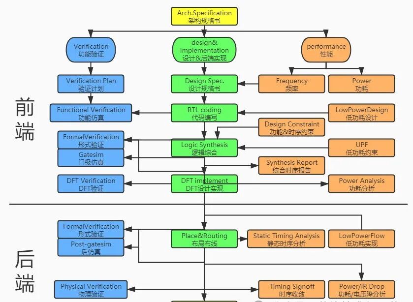
The chip design process is a complex and detailed process that encompasses multiple stages from functional definition to physical layout generation, typically divided into front-end design and back-end design phases.
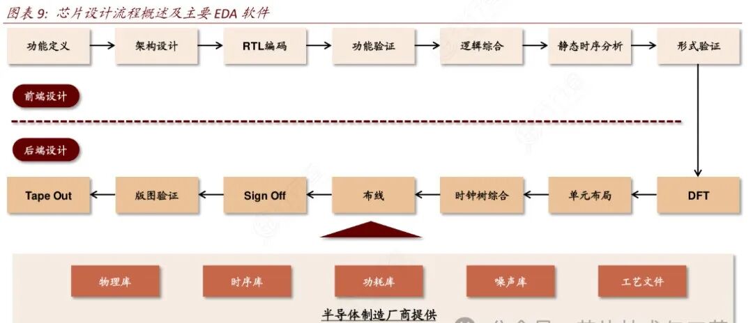
Front-End Design (Front End, also known as Logic Design) is the starting point of chip design, with the main goal of defining the chip’s functionality and architecture. In this phase, the design team conducts detailed requirement analysis, clarifying the specific functions that the chip needs to achieve, and writes RTL (Register Transfer Level) code. The RTL code describes the internal logic structure of the chip, including data paths and control paths, as well as the interaction between various components. To ensure the correctness of the design, the front-end design phase also conducts simulation verification, checking whether the design meets the requirements by simulating the chip’s behavior in actual working environments.
Back-End Design (Backend, also known as Physical Design) unfolds after the front-end design is completed, with the main task of converting the logical description into an actual physical layout. Back-end designers perform layout planning, determining the positions of various functional modules on the chip to optimize performance and reduce power consumption. This is followed by the routing phase, ensuring that signals can be accurately transmitted between modules. Timing analysis and signal integrity analysis are also key stages, ensuring that the chip maintains stable performance under various working conditions. After these steps, the back-end design ultimately generates a complete physical layout, laying the foundation for chip manufacturing.
Close collaboration between front-end and back-end design is key to ensuring the accuracy and reliability of chip design. Front-end designers provide clear and accurate logical descriptions, while back-end designers convert them into efficient physical implementations. Continuous iteration and optimization throughout the design process are essential to ensure that the final chip product meets market demands and performance specifications.
2.2 Preparation Before Tape Out
After the chip design is completed, the intense preparation phase before tape out begins. The work in this phase is crucial as it directly relates to the success of the chip tape out.
- Design Rule Check (DRC): This is the primary step, aimed at verifying whether the design meets the requirements of the manufacturing process. For example, during the layout and routing process, it is essential to ensure that all design elements comply with the size and spacing rules set by the manufacturer to avoid potential manufacturing issues.
- Layout Verification (LVS): This step ensures consistency between the design layout and the schematic by comparing the two, preventing design errors or deviations.
- Parasitic Parameter Extraction: Due to the presence of parasitic parameters such as wire resistance and capacitance, the actual performance of the chip may deviate from the design expectations. Therefore, this phase requires precise extraction of these parasitic parameters and corresponding compensation in the design to ensure that the chip’s performance after tape out meets expectations.
- Communication with Tape Out Manufacturers: Determining specific process parameters, such as doping concentration and oxide layer thickness, which are key factors affecting chip performance. Material selection is also crucial, as the physical and chemical properties of different materials directly impact the performance and reliability of the chip.
- Testing Plan Development: Deciding how to conduct comprehensive performance and reliability testing on the chip after tape out to ensure that it meets design requirements.
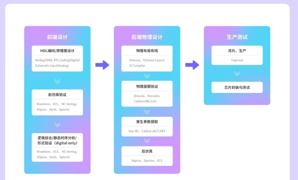
| TypeSubcategory | Description | |
| Front-End Design(Front-End Design) | HDL Coding/Schematic Design | Verilog/HDL RTL Coding (Digital): Writing register transfer level code using hardware description language. Schematic input (Analog): Drawing circuit diagrams using schematic input tools.Schematic input (Analog): Drawing circuit diagrams using schematic input tools. |
| Pre-Simulation Verification | Using simulation tools to verify the functionality of RTL code or schematic, ensuring that the design meets specification requirements. | |
| Logic Synthesis/Static Timing Analysis/Formal Verification | Logic Synthesis: HDL code to gate-level netlist. Static Timing Analysis: Analyzing circuit timing characteristics. Formal Verification: Mathematical methods to prove that the design meets specifications. | |
| Back-End Physical Design(Back-End Design) | Physical Layout and Routing | Using tools to convert gate-level netlist to physical layout and complete routing. |
| Physical Layout Verification | Checking whether the physical layout meets design rules and whether the layout is consistent with the schematic. | |
| Parasitic Parameter Extraction | Extracting parasitic parameters from the physical layout, affecting circuit performance. | |
| Post-Simulation | Simulating design performance considering parasitic parameters. | |
| Manufacturing and Test | Tape Out | Sending the design layout to the wafer foundry for production. |
| Production | Completing cutting, testing, and sorting after wafer production. | |
| Chip Packaging and Testing(Packaging and Testing) | Packaging the chip and conducting functional and performance testing to ensure quality standards. |
Disclaimer: Some articles in this public account are reprinted or adapted from the internet, and the copyright belongs to the original author. However, due to the large number of reprints, it is impossible to confirm the true original author, hence the source is indicated. If there are any copyright issues, please contact us for deletion! 【Cooperation and Consultation】 Please scan the QR code to add staff WeChat (please note the company name)
Click the card below to follow us