#03Detailed Explanation of Chip Fabrication Technology
3.1 Design Check and Layout Verification
Before proceeding with chip fabrication, design checks and layout verification are essential steps that are crucial for ensuring the success of the fabrication process.
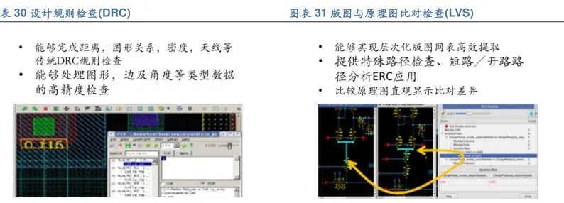
- Design Rule Check (DRC):The main purpose of this process is to conduct a detailed review of the chip layout to confirm that it strictly adheres to manufacturing process rules. This includes checks on critical parameters such as line width, spacing, and layering. Using high-precision software tools, the layout can be automatically scanned to identify any design elements that may violate manufacturing process rules. Once violations are detected, the design team receives immediate feedback for adjustments. This preventive check mechanism significantly improves the yield of chip manufacturing and reduces production risks due to design errors.
- Layout Verification (LVS):This step ensures a high degree of consistency between the chip layout and the original circuit design. Verification tools compare the schematic and layout, checking each component and connection to ensure that the layout accurately reflects the intent of the circuit design, guaranteeing that functionality and performance meet expected standards.
Design checks and layout verification are not one-time tasks. During the design and fabrication process, these two steps may be iterated multiple times to ensure continuous improvement and optimization of the design, with each modification passing through a rigorous verification process. The iterative verification approach enhances the reliability of the design, laying a solid foundation for subsequent chip testing and mass production.
3.2 Layout Routing and Mask (Photomask) Production
Layout routing is a core aspect of chip design, and its complexity is self-evident.In this process, designers must carefully plan each line to ensure it meets functional requirements while achieving optimal performance metrics.
- Signal Integrity:One of the important factors to consider during routing, which relates to whether the chip can stably and accurately transmit signals during actual operation.
- Timing Issues:Reasonable timing design ensures that the chip does not experience timing chaos or signal delays during high-speed operation.
- Power Consumption Control:An increasingly important aspect of modern chip design, effective power management can not only improve the chip’s energy efficiency but also extend its lifespan.
| Figure Name | Content | Remarks |
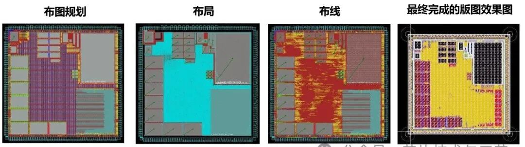
| Completed Layout Planning Effect | The outermost ring is I0PAD, which is the interface connecting the chip to the outside world. The large gray and green modules in the figure are the main IPs. The red and blue lines in the figure are power stripes, used to connect power and ground signals to various components and modules throughout the chip, generally wider. | Layout planning is a crucial step in the entire back-end process, but it is also the most flexible. There is no standard best solution, but many details need to be considered. The goals of layout and routing: optimize chip area, timing convergence, stability, and ease of routing. |
| Completed Layout Effect | The gray and green parts in the figure are the main IPs. The remaining blue parts are standard cells, filled automatically by software. The software will automatically leave appropriate space for the next routing step. | Layout involves placing standard cells, I/O pads, and macro cells to implement circuit logic. The layout goal: the higher the utilization, the better; the shorter the bus length, the better; the faster the timing, the better. However, the higher the utilization, the more difficult the routing; the longer the bus length, the slower the timing. Therefore, a balance among these three parameters must be achieved. |
| Completed Routing Effect | The red and yellow metal lines are automatically routed by software on the standard cells. | Routing refers to connecting each unit and I/O pad with interconnect lines under the constraints of meeting process rules, routing layer limits, line width, line spacing, and ensuring reliable electrical performance of each net. |
| GDSII Effect Layout | Compared to before, this is mainly to meet timing requirements and DRC, LVS requirements, and has re-laid out some areas. Added fillers to meet the density requirements of the metal layer in the design rules. | Clock Tree Synthesis, simply put, is the routing of the clock. Since the clock signal plays a global commanding role in digital chips, its distribution should be symmetrical to each register unit, minimizing clock delay differences from the same clock source to each register. This is why clock signals need to be routed separately. LVS (Layout Vs Schematic) verification: simply put, it is the comparison verification between the layout and the gate-level circuit diagram after logic synthesis; DRC (Design Rule Checking): checks whether the line spacing, line width, etc., meet process requirements; ERC (Electrical Rule Checking): checks for electrical rule violations such as short circuits and open circuits; The actual back-end process also includes circuit power analysis and DFM (Design for Manufacturability) issues arising from continuous advancements in manufacturing processes. The physical layout is delivered in GDSII file format to the chip foundry (referred to as Foundry) to create the actual circuit on the wafer silicon. |
After completing the layout routing, the subsequent mask production step is also crucial.
| Term | Function |
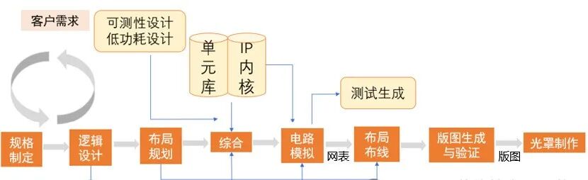
| Customer Requirements | Defines the chip’s functions, performance, interfaces, power requirements, and other detailed specifications, providing guidance for subsequent design work. |
| Design for Testability (DFT) | Considers the testability of the circuit during the design phase to enable effective detection and diagnosis of defects after manufacturing. |
| Design for Low Power (DLP) | Employs specific techniques during the design phase to reduce the chip’s power consumption to meet energy-saving or battery life requirements. |
| Dynamic Test Vector Generation | Generates dynamic test vectors for testing the chip after manufacturing, which will be used during the actual testing phase of the chip. |
| Specification | Defines the chip’s functions, performance, interfaces, power requirements, and other detailed specifications, providing guidance for subsequent design work. |
| Cell Library & IP Cores | Provides the basic building blocks and pre-designed, reusable design components needed for chip design. |
| Logic Design | Uses Hardware Description Language (HDL) to write code that implements the chip’s functional logic. |
| Floorplanning | Determines the location and size of each module on the chip and how they connect, laying the foundation for layout routing. |
| Synthesis | Converts HDL code into a gate-level netlist, which is the process of transforming abstract hardware descriptions into concrete circuit representations. The gate-level netlist details the logic gates and their connections in the circuit, providing input for physical design and timing analysis. |
| Circuit Simulation | Uses simulation tools to simulate the design to verify whether the circuit’s functionality and performance meet expectations. |
| Layout & Routing | Transforms the gate-level netlist into an actual physical layout and completes routing, ensuring correct signal connections on the chip. |
| Mask Generation & Verification | Generates the photomask patterns used for chip manufacturing and verifies that the layout is consistent with design specifications. |
| Mask Making | Produces masks based on the verified layout, which will be used in subsequent chip manufacturing processes for pattern transfer. |
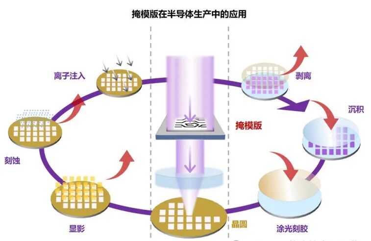
Photomasks, as the bridge that transfers design patterns from the virtual world to real silicon wafers, have their production accuracy directly related to the final quality of the chip.
| Downstream Application MarketField | Product Type | Product Application Field | Downstream Application Representative Manufacturers | Market Share |
| Semiconductor Photomasks | Logic circuit manufacturing, analog circuit manufacturing, power device manufacturing, MEMS sensor manufacturing, IC packaging, etc. | Semiconductor manufacturing industry | Taiwan Semiconductor Manufacturing Company, Intel, SMIC, Hua Hong Semiconductor, China Resources Microelectronics, SMIC Integration, Silan Microelectronics, Jita Semiconductor, BYD Semiconductor, Lian Microelectronics, Yandong Microelectronics, Gaode Infrared, Changdian Technology, etc. | 60% |
| Flat Panel Display Photomasks | LCD display manufacturing, OLED display manufacturing, etc. | Display technology industry | BOE Technology Group, Tianma Microelectronics, Huaxing Optoelectronics, China Electronics Panda, Huike, etc. | 28% |
| PCB (Printed Circuit Board), FPC (Flexible Printed Circuit) manufacturing, touch screen (TP) manufacturing, optical device manufacturing, etc. | PCB manufacturing, touch screen manufacturing, optical device manufacturing, etc. | Electronic manufacturing industry | Lens Technology, ZhiXiang Electronics, etc. | 12% |
Photolithography technology plays a key role in this step, utilizing the principles of diffraction and interference of light to accurately project fine patterns from the layout onto the silicon wafer. Subsequently, through etching and other process steps, these patterns are transformed into actual physical structures, thus completing the chip manufacturing process.
- Increased Routing Density and Complexity:As the integration of chips continues to rise, it presents significant challenges for designers.
- Higher Precision and Efficiency Requirements for Mask Production:As market demands for chip performance continue to increase, mask production faces higher requirements.Overall, layout routing and mask production are indispensable steps in the chip fabrication process, and their technical level and implementation effectiveness directly relate to the final performance and quality of the chip.免责声明:本公众号部分文章系网络转载或改编,版权归原作者所有。但因转载众多,无法确认真正原始作者,故标明转载来源。如涉及版权等问题,请与我们联系删除! 【Cooperation and Consultation】 Please scan the QR code to add the staff’s WeChat (please note the company name)

Click the card below to follow us