Today, we continue to introduce the basics of the plating process in PCB/HDI manufacturing, following Part 2; this is Part 3.
First, let’s introduce a few typical blind hole structures:
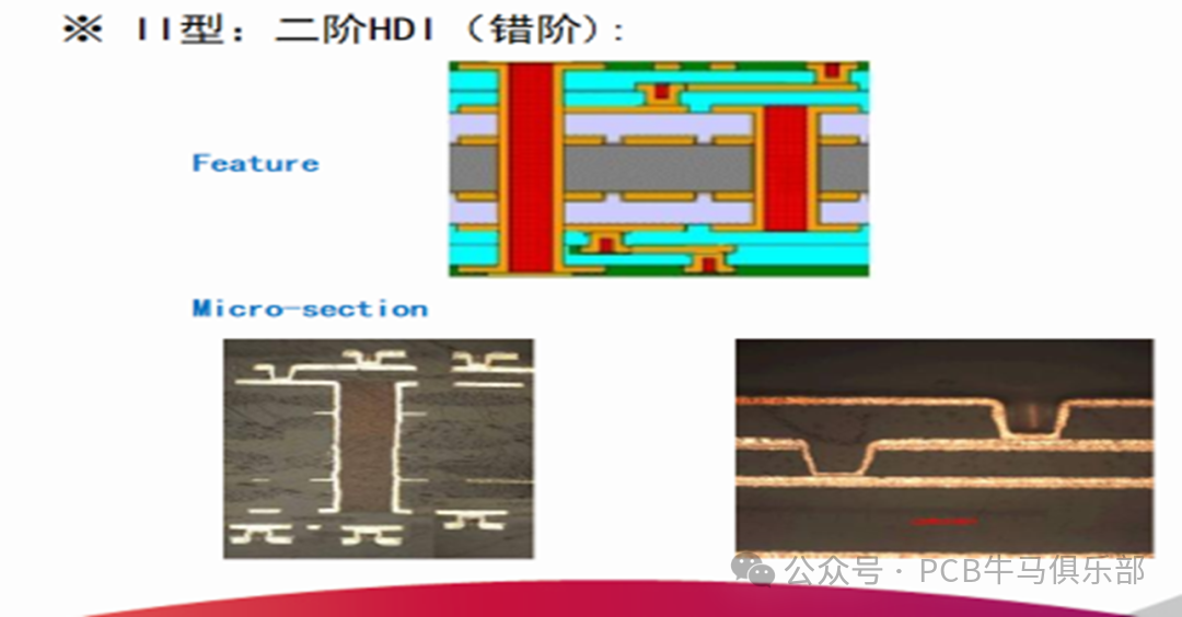
The above case is a 2-layer HDI board with 8 layers, where layers L3-L6 are designed with buried holes, and layers L1/L2, L2/L3 and L6/L7, L7/L8 are designed with 2nd stage blind holes. The blind holes have no stacked hole design, and the customer did not request for the blind holes to be filled.
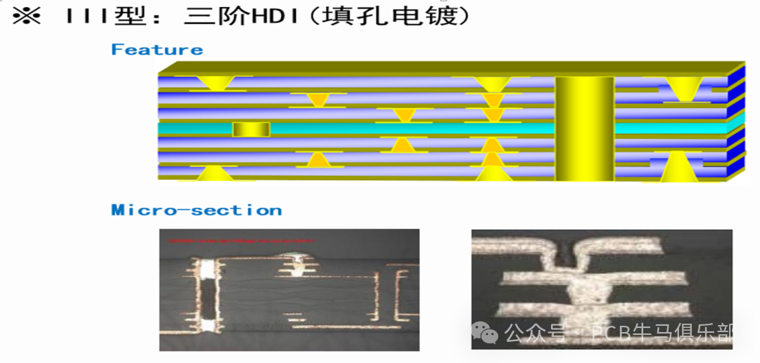
The above case is a 3-layer HDI board, where the inner layer and the next outer layer are designed with stacked holes that need to be filled; the outermost layer does not require the blind holes to be filled as per customer request.
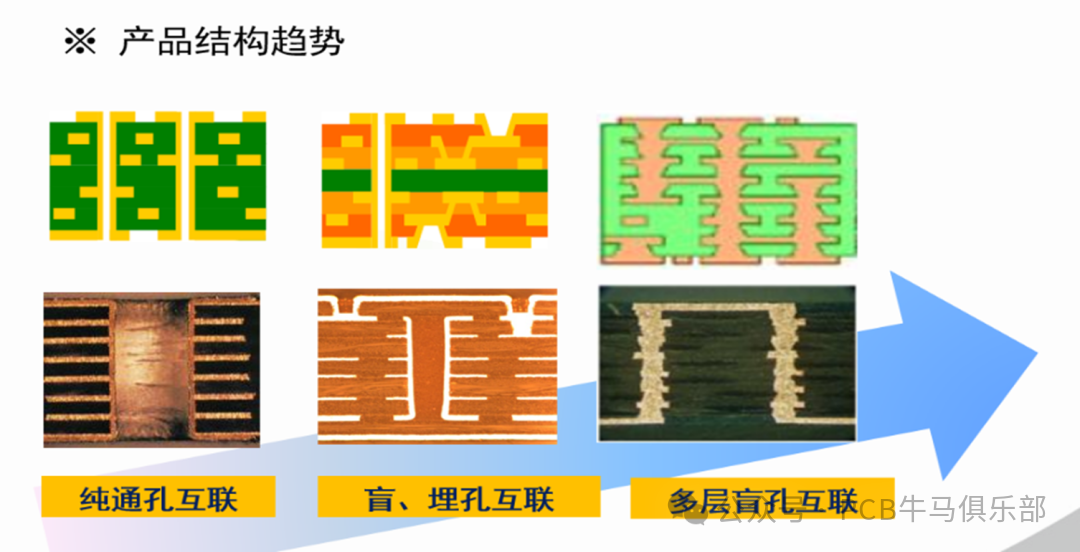
The development direction of HDI boards is any layer interconnection, allowing any two layers in a PCB to be interconnected without restrictions on layer spacing. This greatly enhances the flexibility of routing design and significantly saves PCB area.
4.5.1 Plating (PTH) – Subprocess Function:
Perform overall plating on the completed PTH circuit board to ensure that the copper thickness on the surface and in the holes meets the required standards for subsequent quality demands:
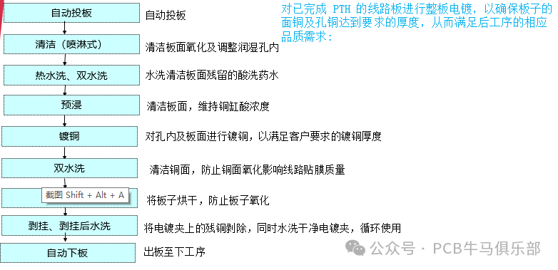
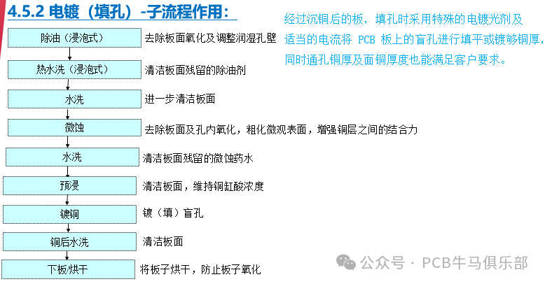
4.5.2 Plating (Filling Holes) – Subprocess Function: Flash plating before filling holes;
After the copper deposition, special plating agents and appropriate current are used to fill or achieve the required copper thickness in the blind holes on the PCB, while ensuring that the thickness of the through-hole copper and surface copper also meets customer requirements.
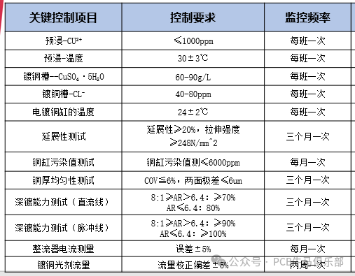
4.5.3 Plating (Through Holes) – Key Control Points:
4.5.4 Plating (Filling Holes) – Key Control Points:
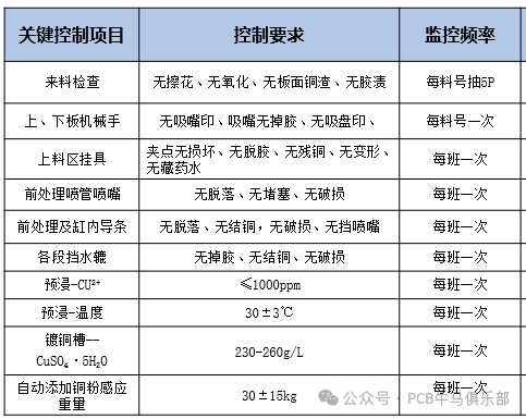
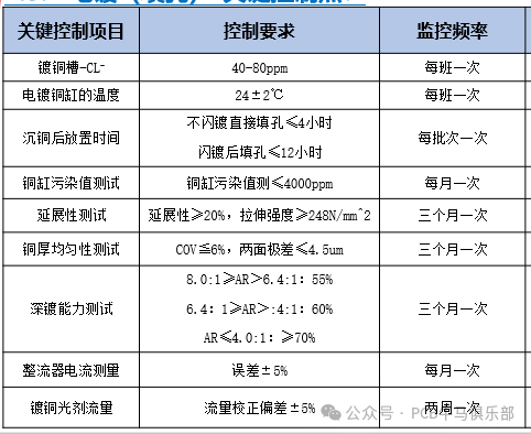
Note: The concentration of sulfuric acid and copper sulfate in filling hole plating is completely different from that in through hole plating, and the differences are significant; the system of plating additives and the principles of plating are also quite different. The main reason is that the plating mechanisms for filling holes and through holes are not the same.
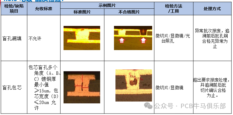
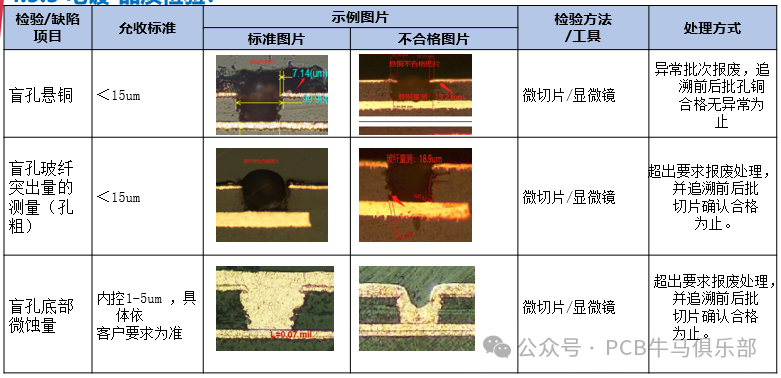
4.5.5 Plating – Quality Inspection:
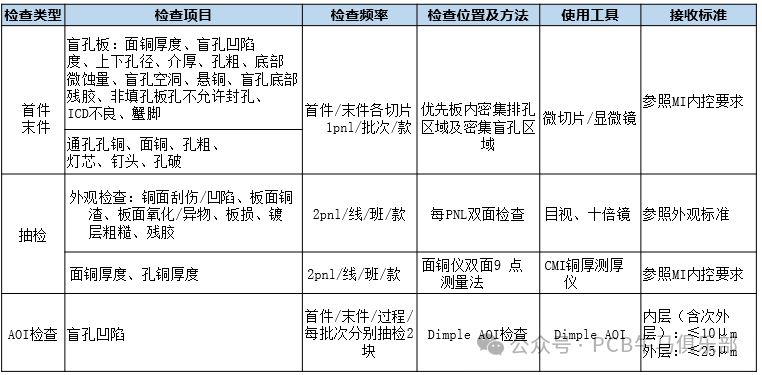
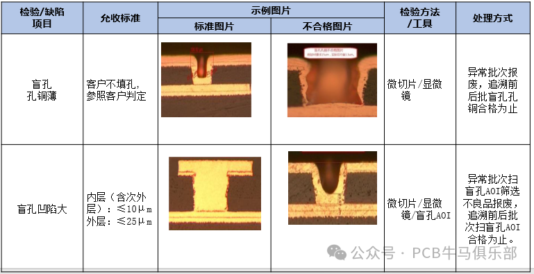
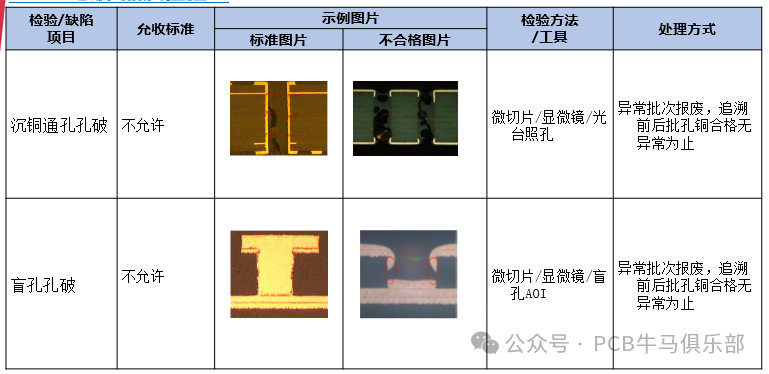
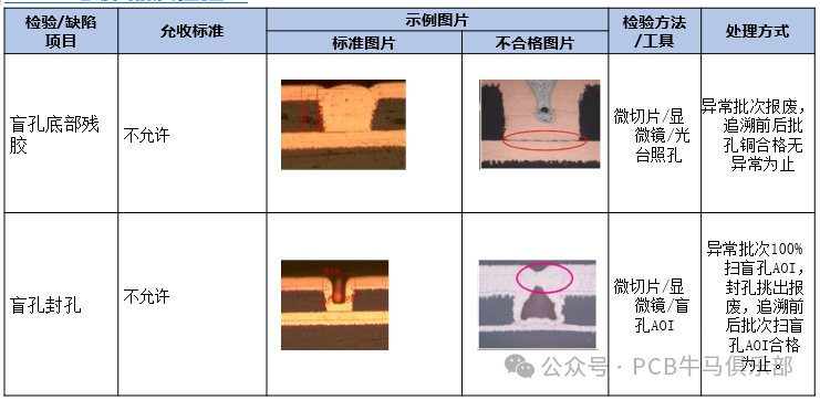
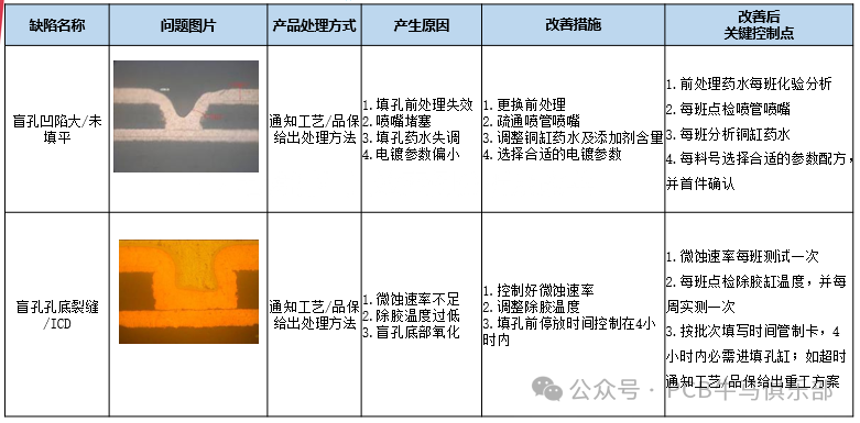
5. Analysis and Improvement of Failure Cases in HDI Plating Process
6. Basic Principles of Copper Plating (Including Through Hole and Blind Hole Plating)
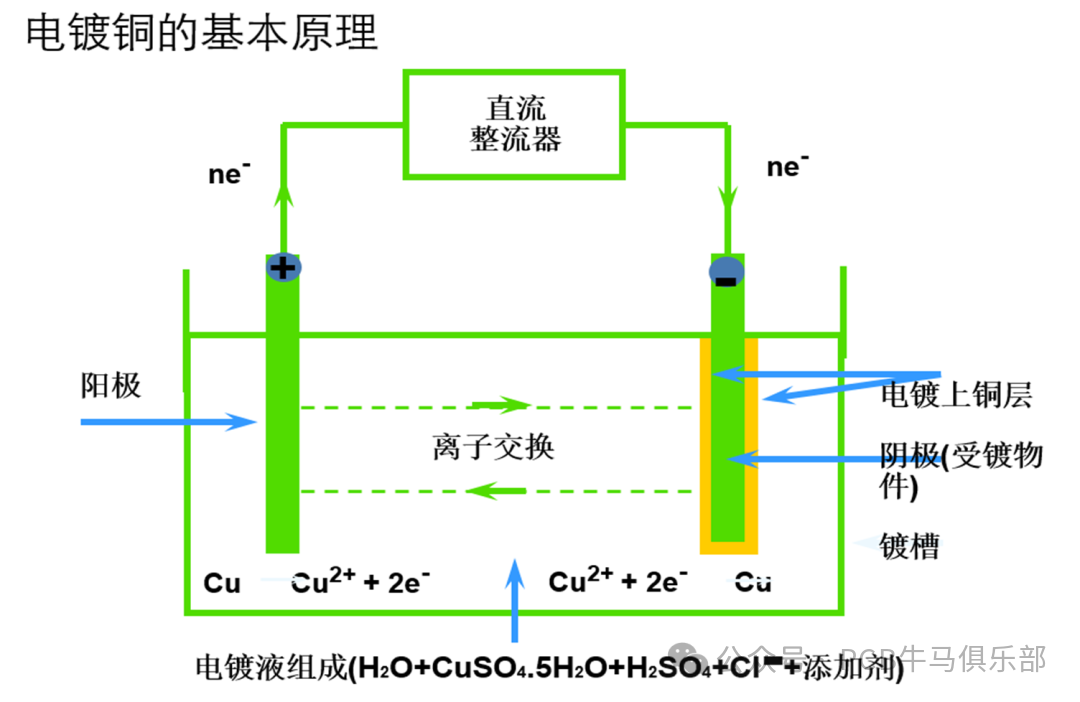
The copper plating solution mainly consists of copper sulfate (CuSO4) and sulfuric acid (H2SO4). Under the influence of direct current voltage, the following reactions occur at the cathode and anode:
Anode (Phosphor Copper Ball/Copper Powder): The phosphor copper ball at the anode is the source of Cu2+ in the copper plating solution. The anode reaction (copper losing electrons and oxidizing) produces Cu2+ in the plating solution as follows:
Cu – 2e = Cu2+
In rare cases, the anode may also undergo the following reaction: Cu – e = Cu+
Cu+ in the plating solution may be oxidized to Cu2+ in the presence of sufficient sulfuric acid and oxygen from the air. When the acidity of the plating solution is insufficient, Cu+ will hydrolyze to Cu2O, forming so-called copper particles/copper powder, which makes the plating rough or spongy, causing burrs or hole blockage. Therefore, it is essential to avoid the generation of cuprous copper during plating.
2Cu+ + 2H2O = 2Cu(OH)2 + 2H+
2Cu+ + 2H2O = Cu2O + 2H
Cathode (Production Board): Cu2+ in the plating solution gains electrons and is reduced to metallic copper.
Cu2+ + 2e = Cu + 0.34V
In some cases, a small amount of Cu+ in the plating solution will also undergo the following reaction: Cu+ + e = Cu
In rare cases, incomplete reduction reactions may occur: Cu2+ + e = Cu+
7. Basic Principles of Filling Hole Plating
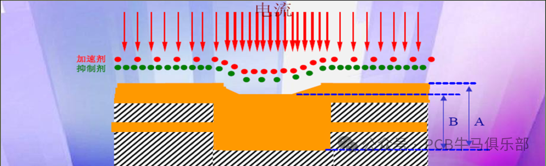
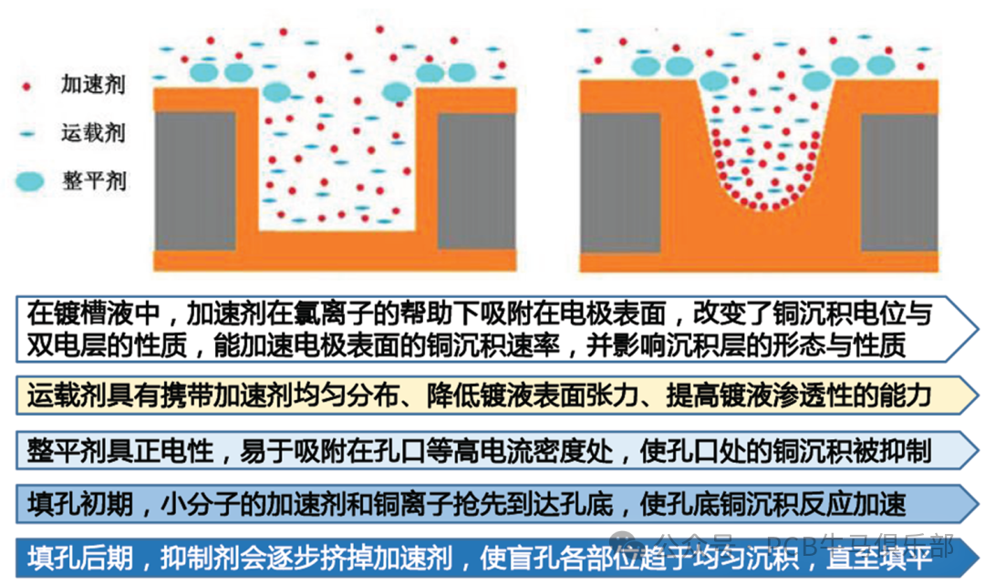
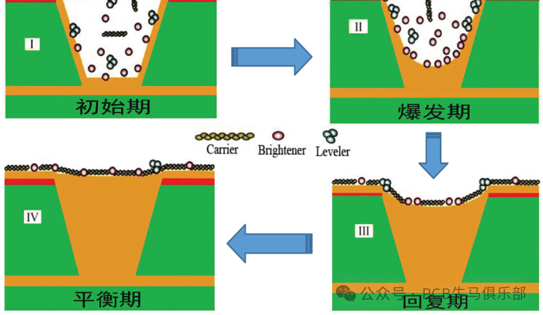
In blind holes, a large number of small molecular brighteners (accelerators) are used, while the board surface uses a large number of large molecular leveling agents (inhibitors), resulting in a copper growth rate in the blind holes that is more than four times that of the surface copper, effectively filling the blind holes. In simple terms, under the action of additives, the copper growth rate inside the blind holes is significantly greater than that of the surface copper, gradually filling the blind holes over time.
8. Schematic Diagram of the Filling Hole Plating Process
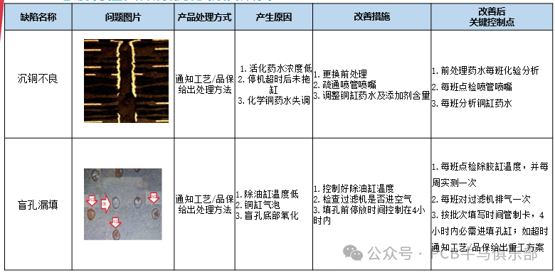
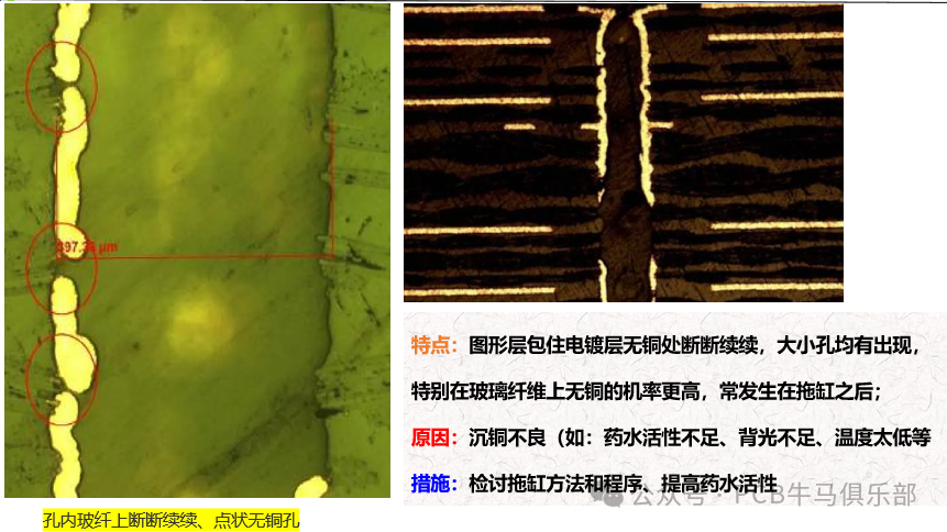
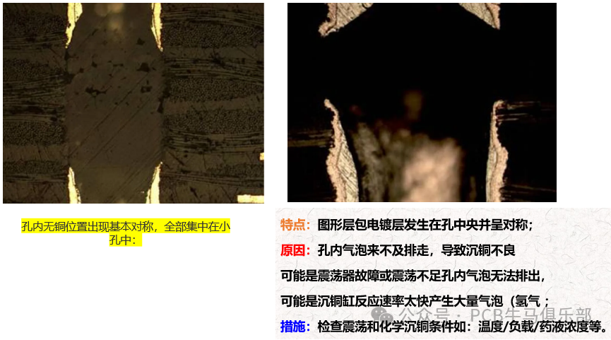
9. Sharing of Two Failure Cases – Poor Copper Deposition
 Special Note: The discussions above are for reference only and serve as a starting point for further exploration! Each factory has differences in chemicals/processes/equipment/product structures, etc., and one must not rigidly apply experiences from one context to another. All effective improvement measures should be based on experimental data! As a professional quality of engineering technicians, it is essential to “speak with data.”
This public account will continue to update information related to PCB manufacturing and cutting-edge technologies.
Thank you for being not only good-looking and handsome but also for using your golden fingers to help us prosper. Please follow, collect, like, share, and leave comments!
Original content is not easy to produce. If you wish to reprint, please privately message the author for consent and indicate the source before reprinting. Thank you for your cooperation!
<img src=”https://mmbiz.qpic.cn/sz_mmbiz_jpg/9A3X8ZaVDBibkC0hT5m4ibkiaSRM5UiaGu5m9tMlibstqRRWHP1vnNlVcQfVnia0CiawBia54geGdKLHHhgJdSPC3wWWTw/640?wx_fmt=jpeg&watermark=1#imgIndex=22″