With the emergence of large models like ChatGPT, DeepSeek, and Gemini, the global demand for computing power has exploded exponentially. While everyone is discussing the shortage of GPU chips, hardware engineers are facing another severe underlying challenge: how to support such an astonishing density of computing power?
The answer lies in those unassuming green circuit boards. The extreme requirements for signal transmission speed, power integrity, and heat dissipation in AI servers are driving a revolution in the PCB industry regarding “layers” and “density.” High-multilayer PCBs and HDI technology have become indispensable “invisible cornerstones” in AI hardware development.

1. Dissecting AI Servers: The “Veins” and “Skeleton” of Computing Beasts
Unlike ordinary servers, the hardware architecture of AI servers is extremely complex. According to a detailed analysis by Guojin Securities, the PCB of a top-tier AI server is mainly divided into three core components: GPU board group, CPU motherboard group, and accessories.
Taking the NVIDIA DGX A100 as an example, it can be roughly divided into five hardware sections:
1. Fan module: The fan module of the DGX A100 consists of 8 fans, which is basically consistent with the traditional 8U specification of servers;
2. Hard drives: Below the fan module is the hard drive and front control panel (for signal transmission with external devices). The DGX A100 is equipped with 8 hard drives of 3.84TB each, totaling 30TB of internal storage;
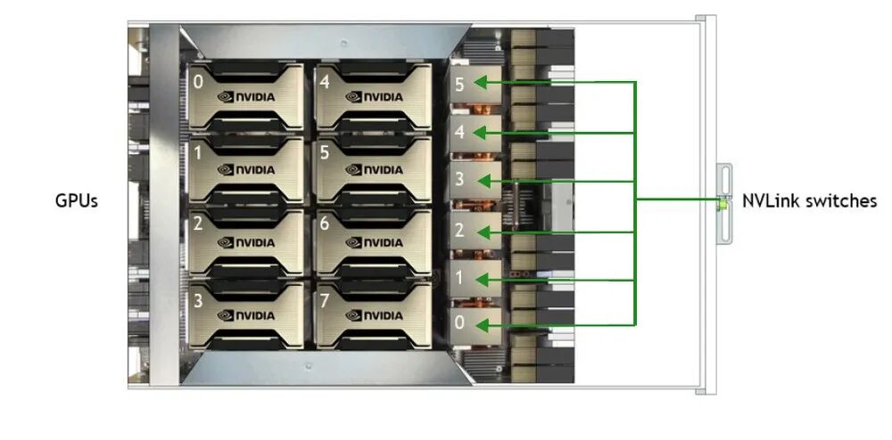
3. GPU board group: The rear section is the key component assembly area of the entire AI server, with the core section being the GPU board group. This is also the key differentiator between AI servers and ordinary servers. From the architecture of the DGX A100, the GPU board group mainly includes GPU components, module boards, and NVSwitch, all of which involve different types of PCB products;
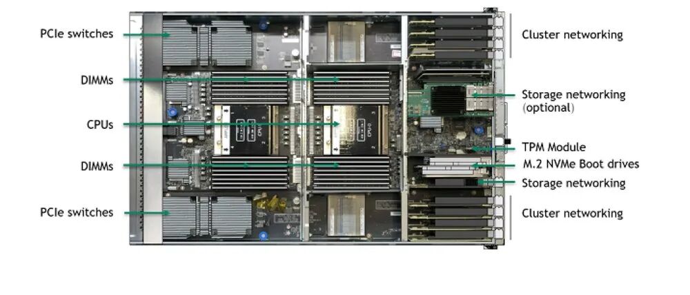
4. CPU motherboard group: This part is the core component of all servers (including both ordinary and AI servers), which includes the CPU motherboard, system memory, network card, PCIe switch, etc. The CPU motherboard, system memory, and network card are the main parts involving PCB usage;
5. Power module: At the rear of the DGX A100, there are also 6 power supply groups, which involve the use of thick copper PCBs.
In terms of value, the PCB value of an ordinary server is about 2425 yuan, while that of a DGX A100 reaches 15321 yuan, an increase of 532%. Among this, 80% of the value increment comes from the GPU board group.
The GPU module board, which supports 8 GPUs, requires a very high number of layers for wiring. In the DGX A100, the GPU module board has an area of about 0.3 square meters and typically requires a 26-layer through-hole board, using Ultra Low Loss materials.
The GPU accelerator card is the core unit that carries the GPU chip. In the DGX H100, the OAM even uses 5th-order HDI technology to meet the extremely high density interconnection requirements between chips.
As for the CPU motherboard, even general-purpose CPU motherboards commonly adopt designs with more than 10-12 layers under the PCIe 5.0/6.0 bus standards, significantly increasing the unit price.
2. Technical Pain Points in High-Multilayer Design and Manufacturing
For hardware development engineers, designing a high-multilayer board for AI applications means overcoming several significant challenges. Even if the design is successfully completed, the manufacturing process faces many challenges. Here are two examples:
1. Extremely Strict Signal Integrity
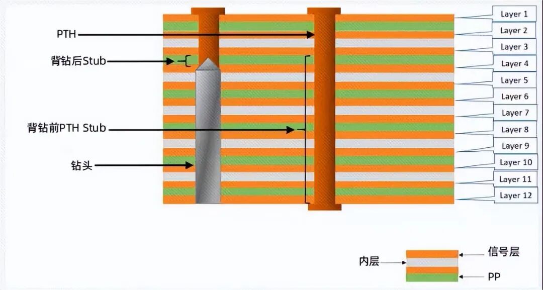
In AI servers, the interconnection of GPUs and PCIe bus speeds are extremely fast. To reduce signal reflection, the manufacturing process of high-multilayer PCBs must use back-drilling technology. Back-drilling refers to the non-through drilling process on one side of the multilayer board to remove unnecessary internal electrical connections. This can eliminate the impact of stubs on signal integrity, ensuring the integrity and impedance continuity of high-frequency signals. For example, Jialichuang has launched back-drilling technology for high-multilayer PCBs, supporting 4-64 layer high-multilayer PCBs. Additionally, impedance must be strictly controlled (usually with an error requirement of ±10% or even lower).
2. Extremely High Aspect Ratio Manufacturing Difficulty
To support high currents and heat dissipation, the thickness of AI server PCBs is usually between 3.0mm and 5.0mm. This results in a very high aspect ratio for drilling. When the mechanical drilling aspect ratio reaches 20:1 (depth/diameter) with a board thickness of 5.0mm, the latest hole diameter is only 0.25mm. This poses a severe challenge for via plating.
3. Breaking Through R&D Barriers: How Jialichuang Uses “High-Multilayer + HDI” One-Stop Solutions to Overcome Technical Barriers
For hardware development engineers, designing a high-multilayer board for AI applications often means facing the triple dilemma of “impossible to make, slow to make, and expensive to make.” Jialichuang leverages its digital manufacturing capabilities to standardize high-multilayer PCBs and HDI boards, providing engineers with new solutions.
1.Breaking Through Layer and Delivery Bottlenecks: From “Waiting for Months” to “Receiving in Weeks”
AI server motherboards often exceed 20 layers, with board thicknesses commonly between 3.0mm and 5.0mm. Traditional factories often require scheduling production for such ultra-high layer orders, with sample delivery times reaching 3-4 weeks, severely slowing down the R&D iteration speed.
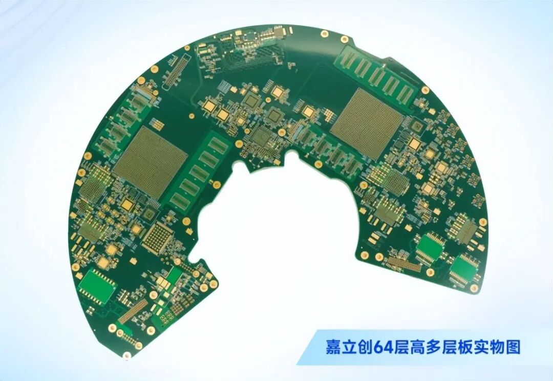
Jialichuang’s current manufacturing capabilities cover 1-64 layers, not only meeting the needs of conventional AI boards but also capable of undertaking extremely complex circuit integration designs in aerospace and other fields. Moreover, through automated production lines and digital processes, Jialichuang has compressed the sample delivery time for high-multilayer boards to 10-15 days, which is twice as fast as the industry average, helping R&D teams seize market opportunities.
2.Overcoming High-Density Interconnection Challenges: The Popularization of HDI and Back-Drilling Technology
AI chips (such as GPUs and switch chips) have extremely high pin densities and must use HDI (High-Density Interconnect) technology. However, advanced HDI processes are complex, and controlling the precision of laser drilling is challenging. Additionally, the back-drilling process required for high-speed signals can easily produce stub residues, affecting signal integrity.
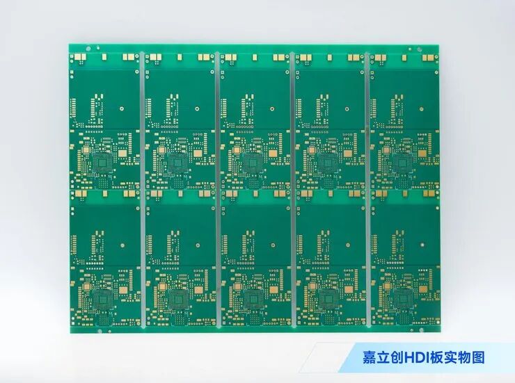
Jialichuang supports 1st to 3rd order HDI blind and buried hole designs, equipped with high-precision laser drilling (minimum hole diameter of 0.075mm) and filling plating processes, perfectly adapting to high-density BGA packaging. At the same time, it provides high-precision back-drilling technology to effectively reduce signal reflection. Additionally, using LDI laser direct imaging technology, inter-layer alignment accuracy can reach 5mil (for ultra-high layers).
3.Reshaping Costs: Making High-Multilayer Prototyping Affordable
High-multilayer boards have high prototyping costs due to low yield and expensive materials. Moreover, any warping or short circuit can lead to the scrapping of expensive AI chips.
Jialichuang’s high-multilayer boards all use high-frequency and high-speed materials such as Shengyi FR-4 S1000-2M (Tg170), ensuring high heat resistance and low expansion coefficients, suitable for the high-temperature conditions of AI servers. Furthermore, thanks to high efficiency, the prototyping cost of high-multilayer boards is about 50% lower than that of peers, greatly reducing the threshold for R&D trial and error.
In Conclusion
The competition for AI computing power ultimately boils down to competition in hardware engineering. When designing the next generation of AI servers, accelerator cards, or high-performance computing units, you no longer need to worry about PCB layer limitations or long delivery times. Jialichuang’s high-multilayer and HDI services are becoming a solid support for your hardware innovation journey with industrial-grade quality, internet speed, and highly competitive prices.