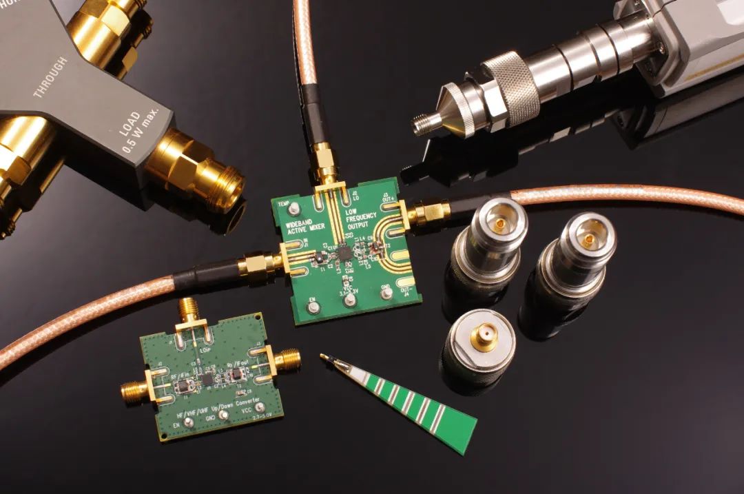
Traditionally, a mobile phone that supports calling, texting, internet services, and APP applications generally consists of five parts: RF part, baseband part, power management, peripherals, and software.
RF: Generally the part for information transmission and reception;
Baseband: Generally the part for information processing;
Power: Generally the part for power saving, as mobile phones are energy-limited devices, so power management is very important;
Peripherals: Generally include LCD, keyboard, casing, etc.;
Software: Generally includes system, drivers, middleware, applications.
In mobile terminals, the most important core components are the RF chip and the baseband chip. The RF chip is responsible for RF transmission and reception, frequency synthesis, and power amplification; the baseband chip is responsible for signal processing and protocol handling. So what is the relationship between the RF chip and the baseband chip?
The Relationship Between RF Chip and Baseband Chip
First, let’s talk about history. RF (Radio Frequency) and baseband both come from direct translations of English. The earliest application of RF was Radio—wireless broadcasting (FM/AM), and this remains the most classic application of RF technology and even in the field of radio.
Baseband refers to signals centered around 0Hz, so baseband is the most fundamental signal. Some also refer to baseband as “unmodulated signals”; this concept was once correct, for example, AM is a modulated signal (no modulation is needed, and the content can be read through sound-generating components after reception).
However, in the field of modern communications, baseband signals typically refer to signals that have undergone digital modulation, with a spectral center point at 0Hz. Moreover, there is no clear concept indicating that baseband must be either analog or digital; it entirely depends on the specific implementation mechanism.
To get to the point, the baseband chip can be considered to include modems, but is not limited to modems; it also includes channel encoding/decoding, source encoding/decoding, and some signaling processing. The RF chip can be viewed as the simplest upconversion and downconversion of baseband modulated signals.
Modulation refers to the process of encoding the signal to be transmitted onto a carrier wave according to certain rules, and demodulation is the reverse process.
Working Principles and Circuit Analysis
RF, short for RF, refers to radio frequency current, which is a type of high-frequency alternating electromagnetic wave, abbreviated from Radio Frequency, indicating electromagnetic frequencies that can radiate into space, with a frequency range of 300KHz to 300GHz. Alternating currents with a frequency of less than 1000 times per second are called low-frequency currents, while those above 10000 times are called high-frequency currents, and RF is such a high-frequency current. High frequency (greater than 10K); RF (300K-300G) is a higher frequency band of high frequency; the microwave frequency band (300M-300G) is a higher frequency band of RF. RF technology is widely used in the field of wireless communication, and cable television systems use RF transmission methods.
The RF chip refers to an electronic component that converts wireless communication signals into certain radio signal waveforms and transmits them through antenna resonance. It includes power amplifiers, low noise amplifiers, and antenna switches. The architecture of the RF chip includes two main parts: the receiving channel and the transmitting channel.
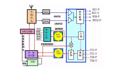
RF Circuit Block Diagram
Structure and Working Principles of the Receiving Circuit
When receiving, the antenna converts the electromagnetic waves sent from the base station into weak alternating current signals, which are filtered and amplified at high frequencies, and then sent to the intermediate frequency for demodulation to obtain the received baseband information (RXI-P, RXI-N, RXQ-P, RXQ-N); sent to the logic audio circuit for further processing.
This circuit focuses on: 1. Structure of the receiving circuit; 2. Functions and roles of each component; 3. Signal reception flow.
1. Circuit Structure
The receiving circuit consists of an antenna, antenna switches, filters, high gain tubes (low noise amplifiers), intermediate frequency integrated blocks (receiving demodulators), etc. Early mobile phones had first and second stage mixing circuits, which aimed to lower the receiving frequency before demodulation (as shown in the figure below).
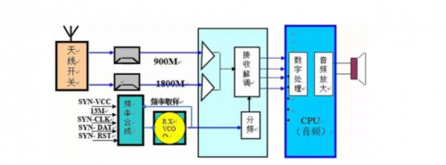
Receiving Circuit Block Diagram
2. Functions and Roles of Each Component
1) Mobile Antenna:
Structure: (as shown in the figure below)
There are two types of mobile antennas: external and internal; composed of an antenna base, helical coil, and plastic casing.
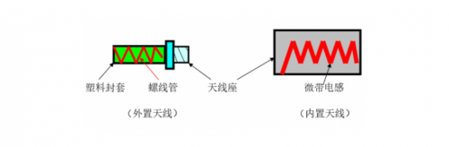
Function: a) During reception, it converts the electromagnetic waves sent from the base station into weak alternating current signals. b) During transmission, it converts the amplified alternating current into electromagnetic wave signals.
2) Antenna Switch:
Structure: (as shown in the figure below)
The mobile antenna switch (combiner, duplexer) is composed of four electronic switches.
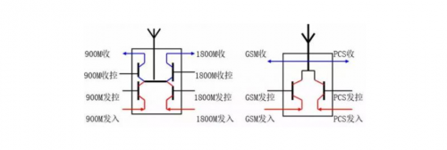
Function: a) Complete the switching between reception and transmission; b) Complete the switching between 900M/1800M signal reception.
The logic circuit sends out control signals (GSM-RX-EN; DCS-RX-EN; GSM-TX-EN; DCS-TX-EN) according to the working status of the mobile phone, allowing each path to conduct, so that the receiving and transmitting signals each follow their own path without interference.
Since the mobile phone cannot receive and transmit simultaneously in one time slot (i.e., it does not transmit while receiving, and does not receive while transmitting), later models of mobile phones removed the two switches in the receiving path, leaving only two transmitting switch; the receiving switching task is handled by the high gain tube.
3) Filter:
Structure: There are high-frequency filters and intermediate frequency filters in mobile phones.
Function: Filter out other useless signals to obtain a pure reception signal. Later models of mobile phones are all zero intermediate frequency phones; therefore, there are no intermediate frequency filters in the phones.
4) High Gain Tube (High Frequency Amplifier, Low Noise Amplifier):
Structure: There are two high gain tubes in mobile phones: a 900M high gain tube and an 1800M high gain tube. They are both common emitter amplifier circuits; later models of mobile phones integrated high gain tubes into the intermediate frequency.
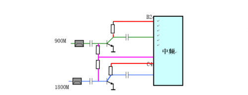
High Frequency Amplifier Power Supply Diagram
Function: a) Amplify the weak current sensed by the antenna to meet the signal amplitude requirements of the subsequent circuit. b) Complete the switching of 900M/1800M receiving signal.
Principle: a) Power Supply: The base bias of the two high gain tubes for 900M/1800M is shared by one path, provided by the intermediate frequency simultaneously; the bias of the collector of the two tubes is sent out in two paths by the intermediate frequency CPU according to the receiving status of the mobile phone; the purpose is to complete the switching of 900M/1800M receiving signal.
b) Principle: The filtered pure 935M-960M receiving signal is coupled through a capacitor and sent to the corresponding high gain tube for amplification, then coupled through a capacitor and sent to the intermediate frequency for further processing.
5) Intermediate Frequency (RF Interface, RF Signal Processor):
Structure: Composed of receiving demodulators, transmitting modulators, transmitting phase detectors, etc.; new models of mobile phones also integrate high gain tubes, frequency synthesis, 26M oscillation, and frequency division circuits internally (as shown in the figure below).
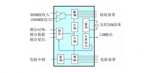
Function:
a) The internal high gain tube amplifies the weak current sensed by the antenna;
b) During reception, it demodulates the received carrier frequency signal (containing the other party’s information) at 935M-960M (GSM) with the local oscillator signal (not containing information) to obtain 67.707KHZ baseband information;
c) During transmission, it modulates the transmission information processed by the logic circuit with the local oscillator signal into the transmission intermediate frequency;
d) Combines 13M/26M crystal to generate a 13M clock (reference clock circuit);
e) According to the reference signal sent by the CPU, it generates a local oscillator signal that meets the mobile phone’s working channel.
3. Receiving Signal Flow
When the mobile phone receives, the antenna converts the electromagnetic waves sent from the base station into weak alternating current signals, which pass through the antenna switch receiving path, are sent to high frequency filters to filter out other useless noise, obtaining pure 935M-960M (GSM) receiving signals, coupled through capacitors and sent to the corresponding high gain tubes for amplification, and sent to the demodulator to demodulate with the local oscillator signal (not containing information) to obtain 67.707KHZ baseband information (RXI-P, RXI-N, RXQ-P, RXQ-N); sent to the logic audio circuit for further processing.
Structure and Working Principles of the Transmitting Circuit
During transmission, the logic circuit processes the transmission baseband information into the transmission intermediate frequency, which is then converted by the TX-VCO into frequency signals of 890M-915M (GSM). After amplification by the power amplifier, it is converted into electromagnetic waves by the antenna.
This circuit focuses on: (1) Circuit structure; (2) Functions and roles of each component; (3) Transmission signal flow.
1. Circuit Structure
The transmitting circuit consists of an internal transmitting modulator, transmitting phase detector; transmitting voltage-controlled oscillator (TX-VCO), power amplifier, power controller, transmitting transformer, etc. (as shown in the figure below).
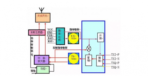
Transmitting Circuit Block Diagram
2. Functions and Roles of Each Component
1) Transmitting Modulator:
Structure: The transmitting modulator is located within the intermediate frequency, equivalent to MOD in broadband networks.
Function: During transmission, it modulates the transmitting baseband information (TXI-P; TXI-N; TXQ-P; TXQ-N) processed by the logic circuit with the local oscillator signal into the transmitting intermediate frequency.
2) Transmitting Voltage-Controlled Oscillator (TX-VCO):
Structure: The transmitting voltage-controlled oscillator is a capacitance three-point oscillation circuit that outputs frequency controlled by voltage; during manufacturing, it is integrated into a small circuit board with five leads: power lead, ground lead, output lead, control lead, and 900M/1800M frequency band switching lead. When there is suitable working voltage, it oscillates and generates the corresponding frequency signal.
Function: Converts the transmitting intermediate frequency signal modulated by the intermediate frequency modulator into frequency signals of 890M-915M (GSM) that can be received by the base station.
Principle: It is well known that base stations can only receive frequency signals of 890M-915M (GSM), while the intermediate frequency signals modulated by the intermediate frequency modulator (e.g., Samsung’s transmitting intermediate frequency signal of 135M) cannot be received by the base station. Therefore, it is necessary to use TX-VCO to convert the frequency of the transmitting intermediate frequency signal to 890M-915M (GSM) frequency signals.
When transmitting, the power supply part sends out 3VTX voltage to enable TX-VCO, generating frequency signals of 890M-915M (GSM) which split into two paths: a) One path samples back to the intermediate frequency, mixing with the local oscillator signal to produce a transmitting phase signal equal to the transmitting intermediate frequency, sent to the phase detector to compare with the transmitting intermediate frequency; if the frequency oscillated by TX-VCO does not match the working channel of the mobile phone, the phase detector will generate a voltage jump (a DC voltage carrying AC transmission information) to control the capacitance of the varactor diode inside TX-VCO, achieving the purpose of frequency accuracy adjustment. b) The other path is sent to the power amplifier, amplified, and then converted into electromagnetic waves by the antenna.
From the above, it can be seen that the frequency produced by TX-VCO is sampled back to the intermediate frequency, and then a voltage is generated to control the operation of TX-VCO; this forms a closed-loop circuit, and is a frequency phase control, thus this circuit is also called a transmitting phase-locked loop circuit.
3) Power Amplifier (PA):
Structure: Currently, mobile phone power amplifiers are dual-band amplifiers (integrating 900M and 1800M amplifiers), divided into black glue amplifiers and iron shell amplifiers; different models of amplifiers cannot be interchanged.
Function: Amplifies the frequency signals output by TX-VCO, obtaining sufficient power current, which is then converted into electromagnetic waves by the antenna.
It is worth noting that the power amplifier amplifies the amplitude of the transmitted frequency signal, but does not amplify its frequency.
Power Amplifier Working Conditions:
a) Operating Voltage (VCC): The power amplifier in the mobile phone is powered directly by the battery (3.6V);
b) Ground Terminal (GND): Forms a return circuit for current;
c) Dual-band Signal (BANDSEL): Controls whether the power amplifier operates at 900M or 1800M;
d) Power Control Signal (PAC): Controls the amplification factor (operating current) of the power amplifier;
e) Input Signal (IN); Output Signal (OUT).
4) Transmitting Transformer:
Structure: Consists of two coils with equal wire diameter and number of turns, placed close together, using the principle of mutual induction.
Function: Samples the power current output by the power amplifier and sends it to the power controller.
Principle: When transmitting, the power current output by the amplifier passes through the transmitting transformer, inducing a current of the same magnitude in the secondary side, which is then detected (high-frequency rectification) and sent to the power controller.
5) Power Level Signal:
The so-called power level refers to the division of the received signal into eight levels by engineers during programming, with each level corresponding to a level of transmission power (as shown in the table below). During operation, the CPU determines the distance between the mobile phone and the base station based on the strength of the received signal, sending out an appropriate transmission level signal to control the amplification factor of the power amplifier (i.e., when reception is strong, transmission is weak).
Attached Power Level Table:

6) Power Controller:
Structure: An operational comparator amplifier.
Function: Compares the sampled signal of the transmission power current with the power level signal, obtaining a suitable voltage signal to control the amplification factor of the power amplifier.
Principle: When transmitting, the power current passes through the transmitting transformer, inducing a current in the secondary side, which is then detected (high-frequency rectification) and sent to the power controller; simultaneously, the pre-set power level signal is also sent to the power controller; after comparing the two signals internally, a voltage signal is generated to control the amplification factor of the power amplifier, ensuring the power amplifier operates at a moderate current, conserving energy and prolonging the lifespan of the power amplifier (higher power control voltage leads to greater power from the amplifier).
3. Transmission Signal Flow
When transmitting, the logic circuit processes the transmitting baseband information (TXI-P; TXI-N; TXQ-P; TXQ-N), sending it to the internal transmitting modulator of the intermediate frequency, which modulates it with the local oscillator signal into the transmitting intermediate frequency. The intermediate frequency signal that the base station cannot receive must be converted by TX-VCO into frequency signals of 890M-915M (GSM) that can be received by the base station. When TX-VCO operates, it generates 890M-915M (GSM) frequency signals that split into two paths:
a) One path samples back to the intermediate frequency, mixing with the local oscillator signal to produce a transmitting phase signal equal to the transmitting intermediate frequency, sent to the phase detector to compare with the transmitting intermediate frequency; if the frequency oscillated by TX-VCO does not match the working channel of the mobile phone, the phase detector will generate a voltage jump to control the capacitance of the varactor diode inside TX-VCO, achieving frequency adjustment. b) The other path is sent to the power amplifier, amplified, and converted into electromagnetic waves by the antenna. To control the amplification factor of the power amplifier, when the power current passes through the transmitting transformer, the induced current in the secondary side is detected and sent to the power controller; simultaneously, the pre-set power level signal is also sent to the power controller; after comparing the two signals internally, a voltage signal is generated to control the amplification factor of the power amplifier, ensuring the power amplifier operates at a moderate current, conserving energy and prolonging the lifespan of the power amplifier.
Current State of Domestic RF Chip Industry Chain
In the RF chip field, the market is mainly dominated by overseas giants, with major companies such as Qorvo, Skyworks, and Broadcom; domestically, no company can independently support the IDM operating model, mainly consisting of Fabless design companies; domestic enterprises form a “soft IDM” operating model through collaboration in design, foundry, and packaging stages.
In terms of RF chip design, domestic companies have made some achievements in 5G chips, with certain shipping capabilities. RF chip design has a high threshold; with RF development experience, subsequent development of advanced RF chip categories can be accelerated. Currently, companies capable of RF chip design include Unisoc, Weijie Chuangxin, Zhongpu Micro, ZTE, Rapoo Technology, Huahong Design, Jiangsu Juxin, Aistek, etc.
In terms of RF chip foundry, Taiwan has become the world’s largest compound semiconductor chip foundry, with major foundries including Win Semiconductors, Advanced Wireless Semiconductor, and Global Unichip. Domestically, only Sanan Optoelectronics and Hawei Huaxin have begun to venture into compound semiconductor foundry. Sanan Optoelectronics has the most comprehensive layout in China, with GaAs HBT/pHEMT and GaN SBD/FET process layouts, currently cooperating with over 200 enterprises and institutions in China, with more than 10 types of chips passing performance verification and about to enter mass production. Hawei Huaxin is a subsidiary of Hitec High-Tech Holdings, in joint venture with China Electronics Technology Group Corporation 29th Research Institute, currently possessing GaAs 0.25um PHEMT process capabilities.
In terms of RF chip packaging, the frequency increase of 5G RF chips leads to a greater impact of the connection lines in the circuit on circuit performance; during packaging, it is necessary to reduce the length of the signal connection lines; on the other hand, it is necessary to package power amplifiers, low noise amplifiers, switches, and filters into a module, reducing size and facilitating use by downstream terminal manufacturers. To minimize parasitic effects of RF parameters, Flip-Chip, Fan-In, and Fan-Out packaging technologies need to be adopted.
Flip-Chip and Fan-In/Fan-Out processes do not require signal connections through gold wire bonding, reducing parasitic electrical effects caused by gold wire bonding and improving the RF performance of the chip; as we enter the 5G era, high-performance Flip-Chip/Fan-In/Fan-Out combined with SIP packaging technology will be the future trend of packaging.

Flip-Chip/Fan-In/Fan-Out and SIP packaging belong to advanced packaging, which has a profitability far higher than traditional packaging. Domestic listed company Changdian Technology, after acquiring Xingshi Jinpeng, has formed a complete Flip-Chip+SIP technology packaging capability.
Note: This article is reproduced from the internet for learning and sharing purposes. If there is any infringement, please contact to delete.
ENDEssential Materials for RF EngineersCommon Knowledge in Huawei Eye DiagramsClassic Books on Antennas (Complete in Chinese and English)Tutorial on Digital Signal Processing👇 Scan to Join the RF WeChat Group, Download Materials for Free 👇