Nand Flash The basic principles have been introduced in my articles from May and August of 2025.
Therefore, we know that when using and programming Nand Flash, the most important aspects are Bad Block management, the use of Spare Area, and the selection of the ECC error checking and correction mechanism.
Before 2015, customers had to fill out surveys for programming Nand Flash because we were concerned that customers might make mistakes in some areas, leading to functionality issues, which made verification and troubleshooting cumbersome. Now, of course, this is no longer necessary as the process has matured, with only a few specific projects still requiring surveys.

Today, we will delve deeper into the usage of Nand Flash regarding Bad Block/Spare Area/ECC through a practical case study from a customer, which happens to cover two programming methods that were not discussed previously.
Customer: ABC
Chip Model: W25N02KVZE
Package: WSON8(8x6mm)
Solution A: Regardless of the reason, the customer could not provide the correct programming file, but they have functional chips OK, which means we can take the W25N02KVZE Nand Flash from the product as a master chip. Can we program it?
è The answer is yes, we can program it. However, since we do not know the algorithm or settings used by the person who programmed this chip, to ensure that the programmed chip functions OK, we should write every byte of the master chip exactly into the slave chip. This understanding is correct, but how do we handle this? Here we need to use the Hard Copy feature of our programmer, also known as hard programming.
There are 3 key points to note when reading (all focused on reading the contents of the master chip without missing a byte).
1. The file must include the Spare Area, which needs to be checked or enabled.
2. Bad Block management needs to ignore bad blocks, meaning bad blocks should also be read.
3. You need to select Not Skip Bad Block, meaning you cannot choose Skip Bad Block.
For example, the reading settings of a programmer from Taiwan are as follows; other programmers operate on the same principle.
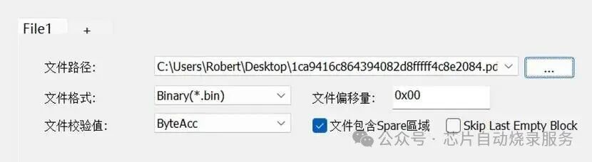
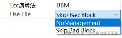
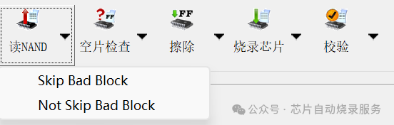
After reading, save the file, and then use the same settings to program the file into the new chip, and it will be OK.
Note: This method of programming chips has a high failure rate because to ensure functionality OK, every byte must match the content of the master chip. Therefore, the new chip cannot have any bad blocks; if there is even one bad block, programming will fail.
Solution B: The above solution A is too cumbersome; reading and saving takes a lot of time, and the failure rate is high. Eventually, the customer provided the programming file through R&D efforts, as shown in the following image.

So how do we program such a file into a chip?
Our programmer supports programming multiple files, but that is inconvenient and prone to errors, leading to batch failures. Therefore, we generally merge multiple files into one for programming. Different programmers have different merging tools, but the best one is Xeltek‘s Partition_merge tool, as shown below:
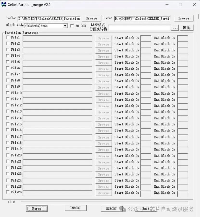
When using this tool, many customers make mistakes in merging files, leading to significant time and effort spent on analysis. Here are a few key issues I remind users about:
1. The selection of Block Mode cannot be arbitrary; you must select the corresponding Block Mode for the chip you are using. For example, for this chip W25N02KVZE, the datasheet states:
The device contains 2048 blocks. Each block contains 64 pages which are divided into 2048 bytes of data area and 128 bytes of spare area.
In simple terms, this chip contains 2048 blocks, each with 64 pages, and each page has 2048 bytes and 128 bytes of spare area.
More concisely, W25N02KVZE= (2048+128) x 64 x 2048 (Byte)
Therefore, the Block Mode for the W25N02KVZE chip should be selected as (2048+128) x 64.
2. Whether to check NO OOB depends on whether the customer’s file contains ECC. You can also directly ask the customer. To analyze whether the customer’s program contains ECC content, I will briefly introduce how to do this. Next time, I will explain the algorithms between different bases in detail. You can use a calculator to convert 2048D=800H, load the file into any programmer’s buffer, and check the address 800 to see if there is any ECC content. If there is, it looks something like this:
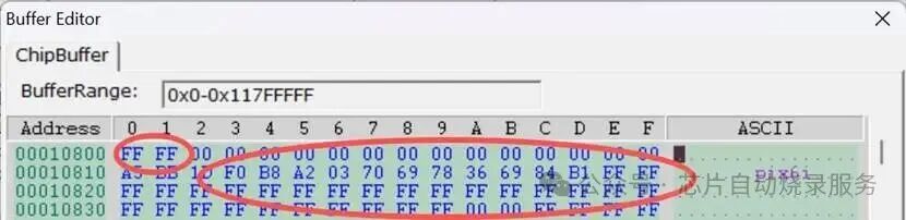
If there is no ECC, it looks something like this:
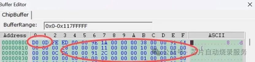
The file provided by the customer this time requires checking NO OOB.
3. Confirm with the customer where each file is programmed to, meaning either provide the starting and ending blocks for each file or specify the address from XXXXXXX to the address XXXXXXX. The principle is the same; the block number and XXXXXXX address can be converted to each other.
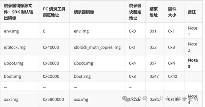
After confirming the above 3 steps, you can correctly merge the data.bin and partitiontable.bin files, returning to the content discussed in August 2025 for correct programming. As follows:
First step: Select the correct chip model.
Second step: Import the corresponding programming file.
Third step: Select the correct ECC method.
Fourth step: Save the project file and click to program.
Learn the basics, understand the underlying logic, and programming is actually very simple!!!