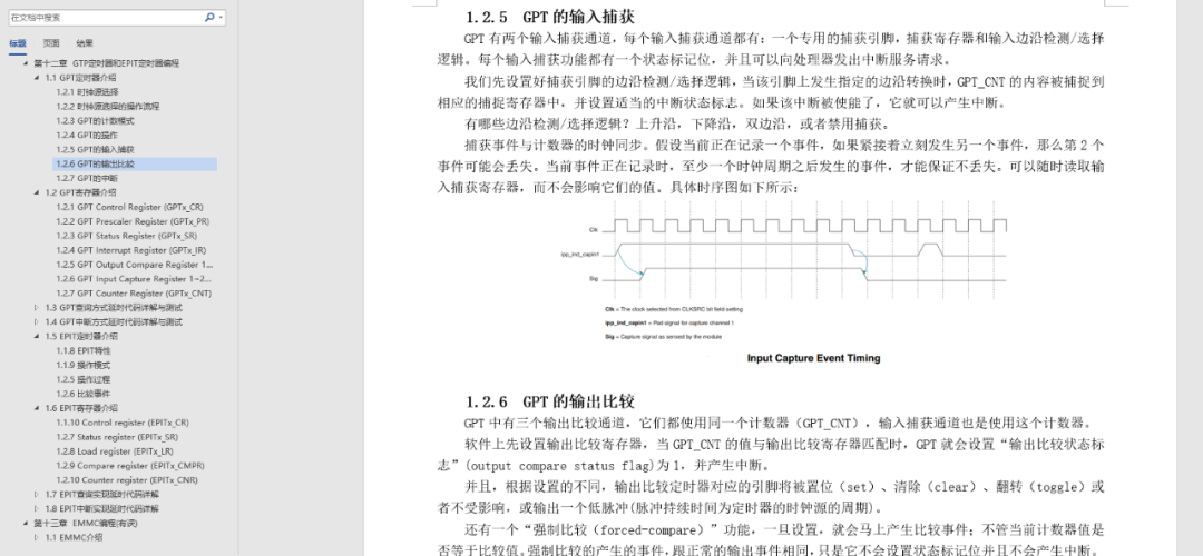
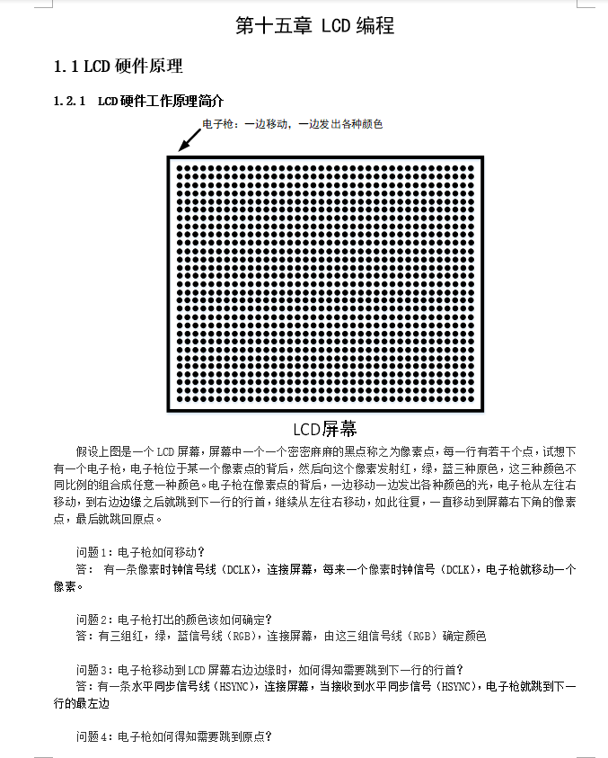
Before we dive into the content, let me announce two things:1. We will publish the progress of the 100ASK_IMX6ULL bare-metal documentation. Writing documentation is not just translating the chip manual, but understanding it and expressing it in simple terms for beginners. The chip manual is written from a foreign perspective, and the writing style is quite different from that of Chinese people. If you don’t understand and just translate it literally, you might as well just look at the English manual. Teacher Wei is currently revising the bare-metal manual, and we expect to release all documentation by this Friday. Below are two screenshots of the revised documents:
2.
Thank you all for your patience. Here is great news: After nearly a month of urgent debugging, the vulnerabilities on the official website (www.100ask.net) have been fixed, and many optimizations have been made. The website is now fully operational.
From now on, customers who purchased videos on Taobao before April 2020 can obtain online viewing redemption codes through the WeChat public account [Baijun Technology] to watch old videos for free (not the upgraded paid videos). The steps are as follows:
1. First, follow this public account [Baijun Technology]
2. Then send a message “redemption code” to the public account, enter the information as prompted to get the redemption code and redeem it.

Below is the main content of this article:
I haven’t worked with NAND Flash drivers for a long time, but recently I’ve been involved again, so I’m summarizing my thoughts. In my opinion, NAND Flash is a relatively outdated storage device, so there aren’t too many details in this article, but rather some development ideas and experiences that I hope can help those in need.
1. Understanding the Current Development Status of NAND Flash
What is NAND Flash?
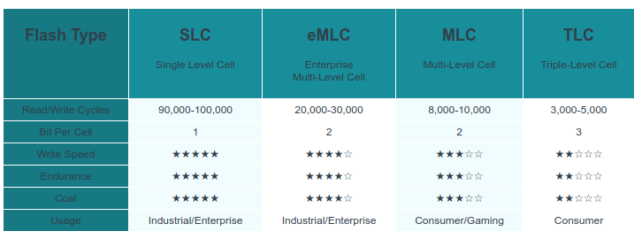
NAND Flash consists of many cells that store bits, which are turned on or off by electric charge. The organization of these on/off cells represents the data stored on the NAND Flash. The number of bits in these cells also determines the naming of NAND Flash, for example, Single Level Cell (SLC) NAND Flash contains one bit per cell. MLC NAND Flash doubles the number of bits per cell, while TLC NAND Flash triples it, paving the way for higher capacity NAND Flash.
The advantage of SLC is its speed and durability, but its downside is its high cost and inability to provide higher storage capacity. SLC is the preferred choice for enterprises. Compared to SLC, MLC and TLC Flash have lower production costs and higher storage capacity, but trade-offs include relatively shorter lifespan and slower read/write speeds. MLC and TLC are the preferred choices for personal items like everyday consumer computers.
Comparison Table of SLC, MLC, and TLC NAND Flash:
Why has eMMC replaced NAND Flash in embedded devices?
Because different brands of NAND Flash chips, including Samsung, KingMax, Toshiba, Hynix, Micron, etc., need to be redesigned based on the product and technical characteristics of each company. In the past, no technology could be universally compatible with all brands of NAND Flash chips.
With each generational shift in NAND Flash process technology, including the evolution from 70nm to 50nm, and then to 40nm or 30nm, mobile customers also need to redesign (what needs to be redesigned? Because communication requires voltage, timing, and even interface commands, all of which differ by manufacturer and process technology. As a mobile manufacturer or SoC vendor, if you want to integrate each new NAND Flash into your product, you need to spend time designing based on these new features. On the SoC side, there will be a NAND Flash controller that you need to configure according to the characteristics of the selected NAND Flash to achieve successful communication).
However, semiconductor products are updated every year, and storage issues also slow down the launch of new mobile models. Therefore, concepts like eMMC, which integrates all storage and the control chip for NAND Flash into one MCP, have gradually become popular. Specifically:
- NAND Flash is a storage medium that requires external control and circuit design to read and write data;
- eMMC is NAND Flash + control IC, with an interface protocol similar to SD and TF cards;
Internally, eMMC fundamentally uses NAND Flash as its storage medium rather than being a completely new storage solution. However, it defines and standardizes interfaces such as eMMC 4.3, 4.4, 4.5 (similar to USB 2.0, 3.0), encapsulating communication with NAND Flash within eMMC while providing an external interface as the eMMC interface. Similarly, externally, for example, the SoC needs to have an SDMMC controller and announce support for eMMC 4.3/4.4, so what you need to do is select a communication interface version number 4.4 based on the selected eMMC version number.
2. How to Drive a NAND Flash?
Reference: “Wei Dongshan’s Embedded Linux Video Episode 1 – NAND Flash”
(1) Basic Hardware Knowledge
NAND Flash is a storage chip, so it should provide the function of “reading data from address A and writing data B to address A”.
Taking the Mini2440 as an example for a brief explanation:
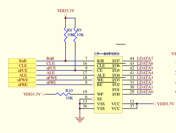
Question 1: The schematic shows only data lines between NAND FLASH and S3C2440; how is the address transmitted?
Answer 1: Data on DATA0 to DATA7 transmits both data and address; when ALE is high, the address is transmitted.
Question 2: According to the NAND FLASH chip manual, commands must be issued to read/write NAND FLASH; how are commands transmitted? On DATA0 to DATA7, data, address, and command are transmitted; when ALE is high, the address is transmitted; when CLE is high, the command is transmitted; when both ALE and CLE are low, data is transmitted;
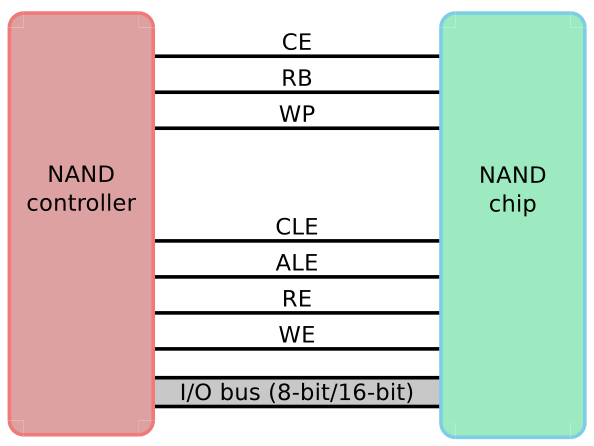
Question 3: The data line LDATAn is connected to NAND FLASH, NOR FLASH, and also to SDRAM, DM9000, etc.; how does the CPU accurately send an address to the correct chip without interfering with others? These chips must be “selected” (i.e., the chip select signal is low) to be accessed; unselected chips will not work, as if they are not connected.
Question 4: Assuming we program the NAND FLASH, after sending commands, addresses, and data to it, NAND FLASH cannot complete programming instantly; how do we determine when programming is finished? By checking the status pin RnB: it is high when ready and low when busy.
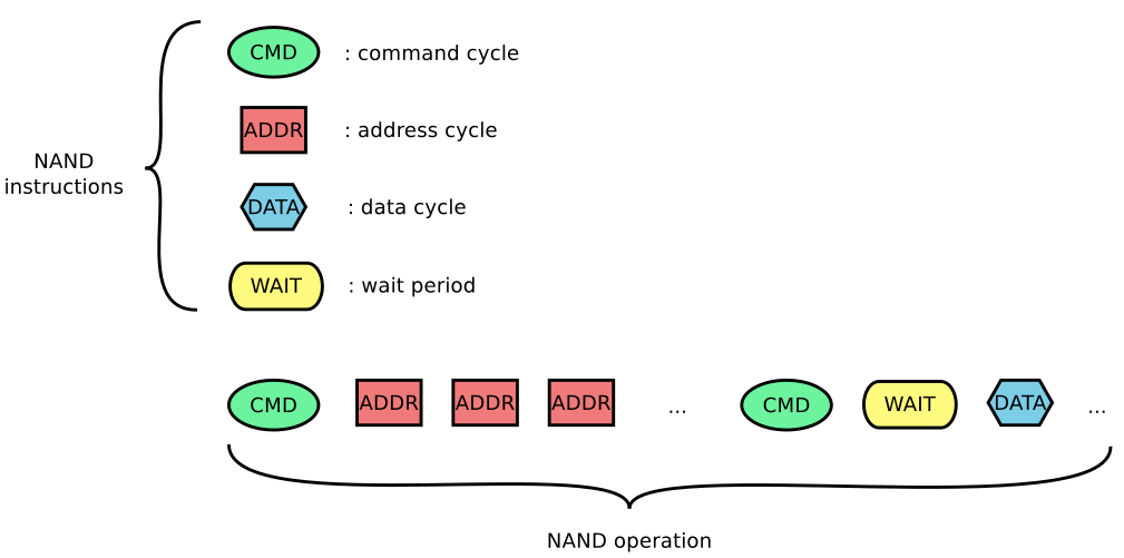
Question 5: How do we operate NAND FLASH? Answer 5: According to the NAND FLASH chip manual, the general process is: (1) Issue command (2) Send address (3) Write data/Read data (4) Wait
(2) CPU NAND Flash Controller Chapter Overview
Using the Samsung S5PV210 chip as an example, here are some important points:
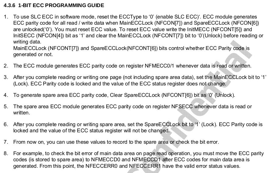
SLC NAND Flash generally uses 1-bit ECC, and the corresponding encoding/decoding process needs to refer to the above content.
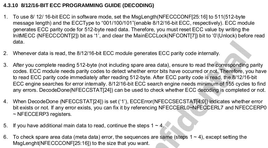
MLC NAND Flash generally uses 8/12/16-bit ECC, and the corresponding encoding/decoding process needs to refer to the above content.
(3) NAND Flash Chip Manual Overview
Using Micron NAND Flash chips as an example, here are some important points:
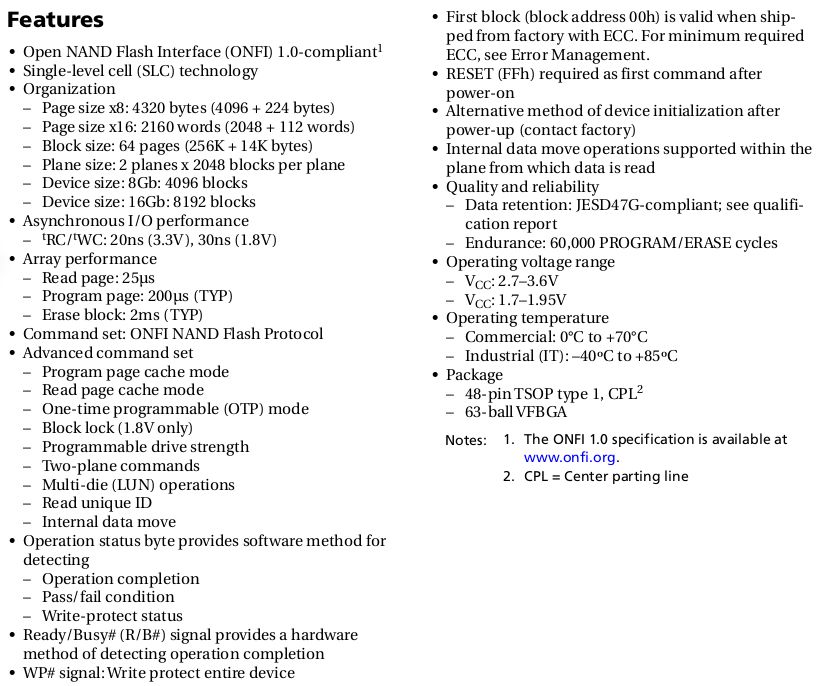
The feature list is usually located on the front page of the chip manual and can help us quickly understand the chip’s characteristics, which can be considered the most important information.
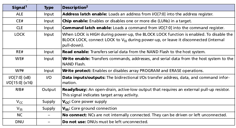
Different chip manufacturers’ NAND Flash pin definitions are generally consistent, but there may be 1-2 pins that differ and need to be checked.
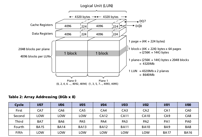
The above image can be used to determine the storage layout of NAND Flash;
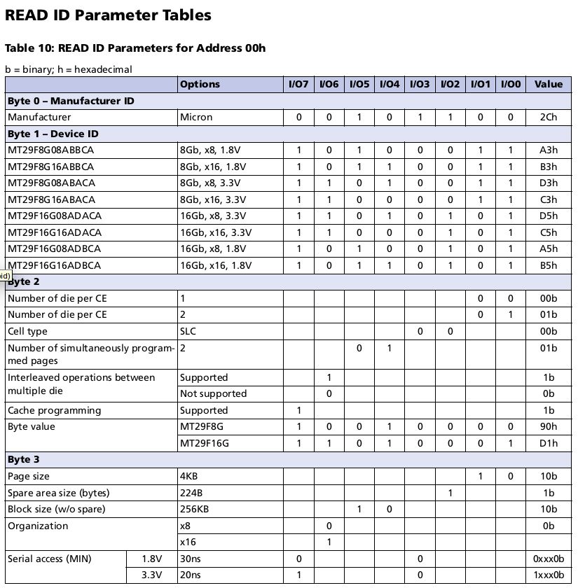
The above image can be used to verify the chip model and detailed hardware characteristics;
(4) NAND Flash Debugging Ideas:
1. Thoroughly read the CPU chip manual’s NAND Flash controller section:– Understand what features the CPU NAND Flash controller supports, generally including the bit count of NAND Flash, to determine if it supports the currently selected NAND Flash chip; – Clarify the workflow of the NAND Flash controller’s ECC verification function;
2. Read the NAND Flash chip manual thoroughly:– Understand the basic information of the NAND Flash chip, such as ID, capacity, type (SLC/MLC). – View it together with the board’s schematic to ensure that the pin connections between the CPU and NAND Flash chip are correct. Different manufacturers (e.g., Samsung, Micron) may not have fully compatible NAND Flash pins, and there may be one or two pins that differ;
3. Implement the function to read the ID value of the NAND Flash chip in U-boot or Linux: nand_read_id()– Use U-boot or Linux as convenient; U-boot’s advantage is quick startup, making testing easier, while Linux’s advantage is support for networking/file systems and powerful functionality; – Being able to read the ID only indicates that there is some assurance of the hardware connection between the CPU and NAND Flash chip (e.g., issuing commands, reading data), but certain hidden errors in hardware connections can still lead to abnormal data writing;
4. Implement the function to read and erase a data block in U-boot or Linux: nand_erase_block()– Compared to reading and writing data, erasing a NAND Flash data block is relatively easier. Moreover, only after successfully erasing can we further verify the read/write functionality of NAND Flash. After a NAND Flash data block is erased, all data is 0xFF, using this feature to verify whether the later implemented read one page operation is normal;
5. Implement the function to read raw data from one page (ignoring ECC verification) in U-boot or Linux: nand_read_page_raw()– One page of NAND Flash includes the main area and OOB area; the main area is for storing user data, and the spare area is for storing ECC verification codes; – Generally, when writing one page of data, context is needed to determine whether to write to the main area or to the main + spare area; – NAND Flash generally requires ECC verification functionality to ensure data safety, but in the early debugging phase, we can implement the function to read raw data from one page without considering ECC verification. In fact, we cannot consider ECC verification functionality yet, as we still cannot write data to the main area of NAND Flash, let alone write ECC verification codes to the OOB area; – We need to implement the data reading functionality first, ensuring its reliability before we can use it to verify the data writing operation;
6. Implement the function to write raw data to one page (ignoring ECC verification): nand_write_page_raw()– Raw writing one page and raw reading one page operations can mutually verify each other; – The cmp command in U-boot can compare whether the data in two memory blocks is the same, and this command can be used to verify whether the write operation is successful;
7. Implement the function to write one page of data to the main area and fill the ECC verification code generated by the NAND Flash controller into the OOB area: nand_write_page()– When writing one page of data to the main area, the NAND Flash controller generates ECC verification codes, which are used to protect the data of that page;
8. Implement the function to read one page of data, including reading the main area data and the spare area ECC verification code: nand_read_page()– The ECC verification code read from the NAND Flash spare area should be sent to the NAND Flash controller, which will help us calculate whether there are bit errors and store the results and information needed for error correction in registers, allowing software to deduce the correct data from the information in the registers;
9. Since bit error issues are not easily encountered, during the debugging phase it is necessary to artificially create mismatched main data with the spare area to verify whether the ECC verification functionality is normal, i.e., whether the data can be corrected. The general idea is:– Write one page of correct data to the main area and spare area using nand_write_page(); – Tamper with the data in memory, then use nand_write_page_raw() to fill the tampered data into the main area while keeping the spare area unchanged; – Use nand_read_page to read one page of data; if it can execute the error correction-related code and retrieve the data before tampering, it indicates that the verification function is working;
10. If the number of ECC verification code bytes in the main area is large enough and the spare area is large enough, a second ECC can be applied to the main ECC verification code stored in the spare area. The ECC generated in this case is referred to as spare ECC, which is generally stored at the end of the spare area but is not mandatory;
(5) Linux NAND Flash Driver
Reference: “Wei Dongshan’s Embedded Linux Video Episode 2 – NAND Flash”
Linux MTD stack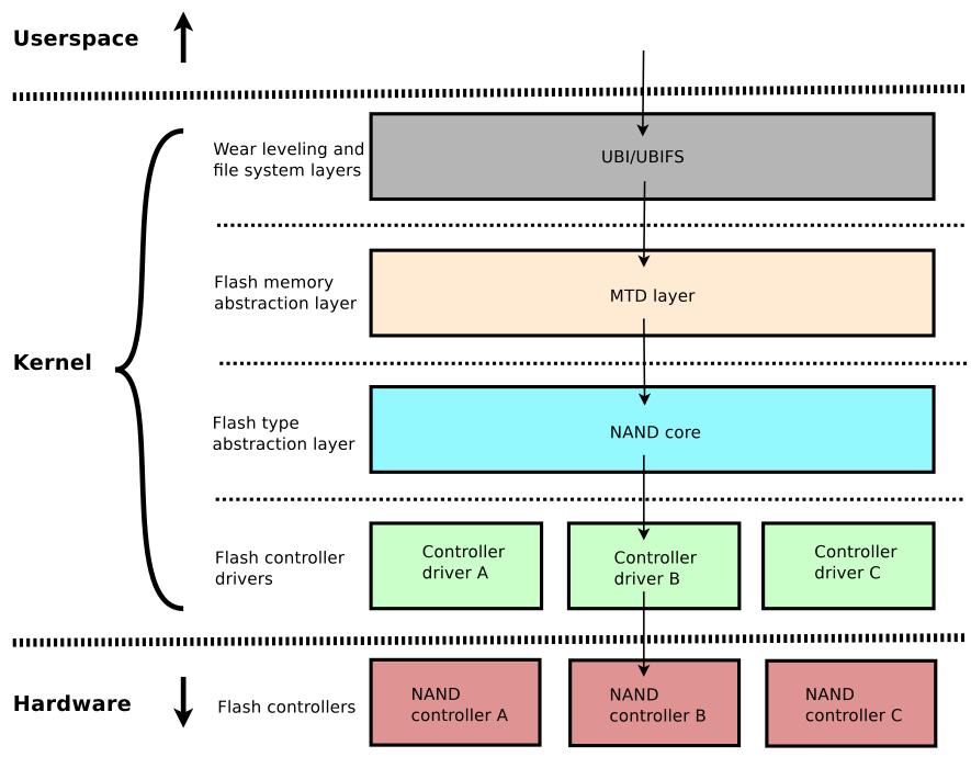
For NAND Flash drivers, the key areas to focus on are:
Flash memory abstraction layer/MTD layer drivers/mtd/mtd*.c Flash type abstraction layer/NAND core drivers/mtd/nand/nand_*.c Flash controller drivers drivers/mtd/nand/*_nand.cNAND Legacy Stack (before Linux-4.16)
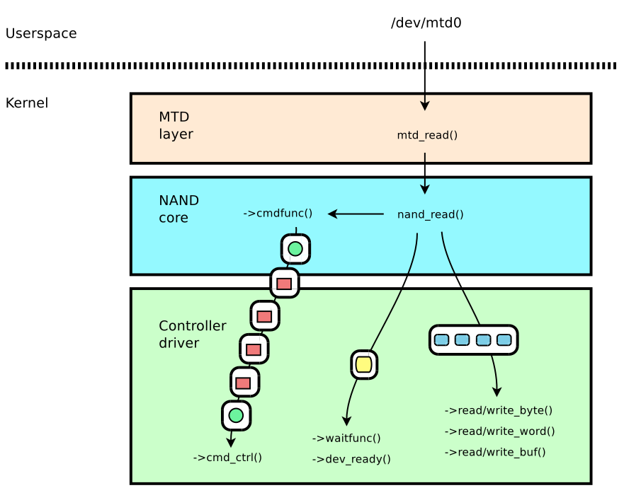
/dev/mtd0 is the character device driver node for the NAND Flash device, and the above image shows the low-level implementation of read(“/dev/mtd0”) (MTD layer -> NAND core -> Controller driver).
The drawbacks of the NAND Legacy Stack
- Unable to execute fine-grained NAND Flash commands, as the granularity is limited to the NAND core level;
- When chip manufacturers update NAND Flash features, all Controller drivers need to be modified;
NAND New Stack (after Linux-4.16)
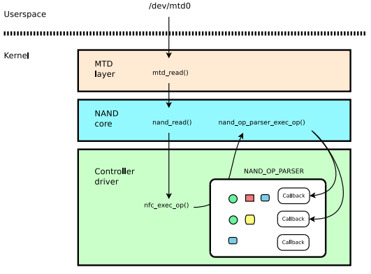
The control logic of NAND is delegated to the Controller driver level, with the NAND Core uniformly calling the hook function provided by the Controller driver: exec_op();
(6) Testing Stability and Performance
MTD Tests Support
- mtd_nandecctest.ko: NAND Flash ECC verification test
- mtd_pagetest.ko: NAND Flash page read/write test
- mtd_speedtest.ko: Read/write speed test of MTD partitions
- mtd_subpagetest.ko: NAND Flash sub-page interface test
- mtd_oobtest.ko: NAND Flash OOB area read/write test
- mtd_readtest.ko: Read the entire MTD partition
- mtd_stresstest.ko: Random read/write and erase operation test
- mtd_torturetest.ko: This function can be used for stability or lifespan testing, performing random operations until an error occurs
Example as follows:
insmod mtd_stresstest.ko dev=9 count=1000 [ 3289.273771] ================================================= [ 3289.279826] mtd_stresstest: MTD device: 9 [ 3289.284079] mtd_stresstest: MTD device size 268435456, eraseblock size 131072, page size 2048, count of eraseblocks 2048, pages per eraseblock 64, OOB size 64 [ 3289.303250] mtd_stresstest: scanning for bad eraseblocks [ 3289.420267] mtd_stresstest: scanned 2048 eraseblocks, 0 are bad [ 3289.426534] mtd_stresstest: doing operations [ 3289.431031] mtd_stresstest: 0 operations done [ 3339.606972] mtd_stresstest: finished, 1000 operations done [ 3339.612992] =================================================A small script for repeatedly reading and verifying data correctness:
#!/bin/sh rm -rf /media/local/ count=1 while [ ${count} -lt 600 ]; do TSTAMP="`date` | ---> ${count}" echo "$TSTAMP" mkdir -p /media time cp /usr/local /media/ -raf diff /usr/local /media/local -r || exit -1 rm -rf /media/local; sync let count=${count}+1 done3. Choosing a File System for NAND Flash: YAFFS2
Reference: “Organizing File Systems Based on NAND Flash” “Comprehensive Comparison of Cramfs, JFFS2, YAFFS2”
Optimizing performance for NAND Flash characteristics and overcoming its disadvantages
-
NAND Flash is not a typical block device; block devices can perform read/write operations on data blocks (like disks, file systems, etc.), but for NAND Flash, there are three operations: read, write, and erase. Write operations can only be performed on erased blocks. Therefore, to make it compatible with traditional hardware and systems, special handling is required;
-
When a flash memory is in a clean state (erased but no write operations have occurred), every bit on this flash is logically 1;
-
The lifespan of flash memory is limited, specifically determined by the maximum number of erasable times for erase blocks. If the maximum erasable times are exceeded, that erase block becomes a bad block. Therefore, to avoid overusing a certain erase block, which would cause it to become a bad block before others, write/erase operations should be evenly distributed across each erase block with minimal impact on performance, known as wear leveling.
YAFFS stands for “Yet Another Flash File System” and is currently the only file system specifically designed for NAND Flash. It uses a log-structured approach, combined with the characteristics of NAND Flash, providing wear leveling and power loss protection mechanisms that effectively avoid the impact of unexpected power loss on file system consistency and integrity.
How do NAND Flash and YAFFS2 work together? By analyzing mkyaffs2iamge.c, we can see:
- YAFFS2 image files consist of individual main (4096) + spare (224) data;
- The main area stores file data (including directories, regular files, special files, etc.);
- In the spare area, the first nand_oobinfo->oobfree (2+22=24) bytes are free for YAFFS2 use, and the subsequent nand_oobinfo->eccbytes (104) bytes are filled with 0xFF, meaning that YAFFS2 images do not contain ECC verification codes; (the above values are related to the actual NAND Flash chip)
More details: how-yaffs-works[1]
References
[1]
YAFF2 Official Website: https://yaffs.net/documents/how-yaffs-works
﹀
﹀
﹀
Recommended Hot Articles:
Wei Dongshan: Specifying Interrupts in Device Trees – Obtaining Interrupts in Code
Wei Dongshan: Analyzing Important Data Structures in the Linux Interrupt System
Wei Dongshan: Porting Kernel Drivers to Use Six-Axis Sensor ICM20608 on 100ask_imx6ull
Wei Dongshan: A Comprehensive Look at the History of Interrupt Handling in Linux
Wei Dongshan: Supporting Other Models of Screens on the 100ASK_IMX6ULL Board
Discussing Several Core Issues of UBOOT
You can also join the discussion group: