RS-485, what does RS mean? It is an abbreviation for Recommended Standard, which means a recommended standard. 485 is the standard identification number, and there is no need to delve into why this identification number is set. RS-485 is also known as ANSI/TIA/EIA-485, these prefixes are abbreviations of standard associations’ names, for example, EIA stands for Electronics Industries Association. In 1983, the RS-485 communication interface was approved by the Electronics Industries Association as a communication interface standard.Even today, in the hot IoT era, RS-485 still has a large number of applications. Many protocols use RS-485 as the physical layer. For example, what are the commonly used standard protocols that use RS-485 as the physical layer? For example:
Industrial HART Bus
Modbus Protocol
Profibus DP
…….
Electrical Characteristics
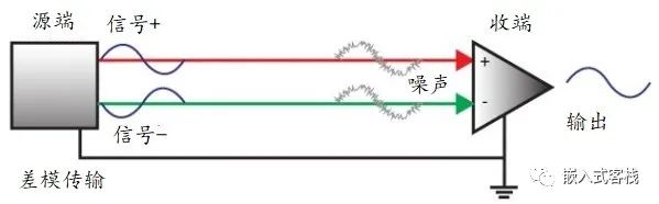
Signal sampling uses differential mode transmission, which is relative to common mode; differential mode is also called differential. So what kind of transmission is differential mode? A picture is worth a thousand words; just look at the two diagrams below:
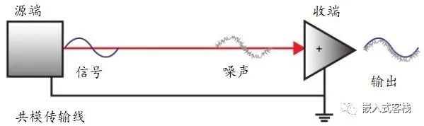
Common Mode Transmission
When using common mode transmission, common mode noise will superimpose on the final output signal, contaminating the original signal.
Differential Mode Transmission
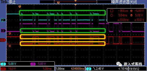
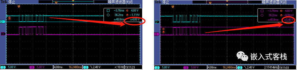
In differential mode transmission, the signals + and – emitted from the source are out of phase. For common mode noise, it exists on both + and – lines. In an ideal situation, they have equal amplitude and the receiver acts like a subtractor. The useful signal, due to the opposite phase, is retained after subtraction, while the noise is canceled. In actual circuits, it is significantly weakened.Thus, it can be seen that differential mode transmission has an advantage over common mode transmission in effectively canceling common mode interference.Differential mode is also referred to as balanced mode in some places, while common mode is referred to as unbalanced mode.To observe this interference, let’s take a look at a waveform:At the edges of signals A/B, the waveform is slightly distorted, but when you see A-B difference (the red line is the oscilloscope’s MATH subtraction function, for A-B), the edges become very clean! This example illustrates that differential mode transmission can effectively resist common mode interference.
Electrical Parameters
The electrical parameters of RS-485 are:
Common mode voltage range is -7 to +12V
Supports up to 32 multipoint topology connections, see the network topology diagram below
Using a 40-foot cable, the transmission rate can reach 10Mbps, where 1 foot is equivalent to 30.48 cm, and Mbps means megabits per second
Using a 4000-foot cable, the transmission rate can reach 100kbps
Half-duplex Communication
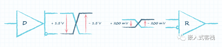
Minimum differential voltage tolerance: 200mV, meaning that the receiver cannot correctly identify 0/1 when the differential voltage is below 200mV. How should this be understood?
How should the above diagram be understood? The RS-485 transceiver’s sending circuit must provide at least 1.5V differential voltage output capability. Due to bus line impedance attenuation, 32 receiver circuit input impedances, and 120Ω termination resistance, the differential signal amplitude will gradually attenuate. Therefore, at the end, at least 200mV of differential voltage must be provided to the terminal receiving circuit.
: For the receiving circuit, it determines the difference between the common mode voltage of wire A and wire B:
If , the receiving circuit R identifies it as logic 1
If , the receiving circuit R identifies it as logic 0
In simple terms, if the absolute voltage value of wire A is at least greater than 200mV than that of wire B, it is identified as logic 1; or if the absolute voltage value of wire A is at least less than 200mV than that of wire B, it is identified as logic 0
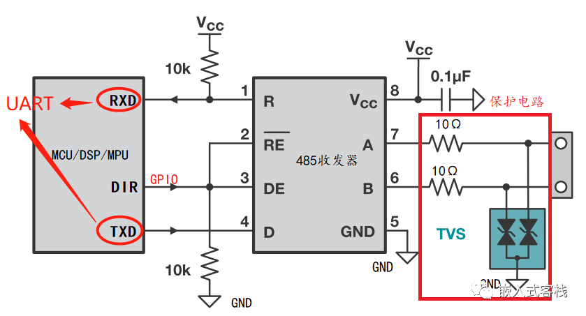
The parameters here should be theoretical values under certain characteristic impedance lines, and adjustments and on-site testing are required during actual engineering use. It is generally advisable not to exceed these theoretical limits.Speaking of electrical characteristic parameters, let’s first look at a general interface circuit:From this interface circuit, there are several key points:
From the perspective of RS-485 communication, the microcontroller/DSP/processor interface uses the UART interface with the RS-485 transceiver interface. Of course, you may ask if I can use FPGA? Certainly, it is possible to implement a serial transceiver IP module with FPGA. Even if you want to say, can I simulate UART with GPIO? That is also feasible, but it is not very meaningful and requires CPU resources to implement the low-level BIT transmission.
Earlier we mentioned half-duplex; where there is half-duplex, there is full-duplex. What is half-duplex? First, half-duplex and full-duplex are defined in a point-to-point manner. Here point-to-point means at the same time. Half-duplex means that the device can either be in data receiving state or data transmitting state at the same time, but not both.
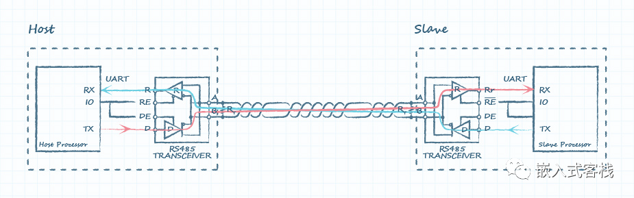
Full-duplex, on the other hand, allows simultaneous transmission and reception. For example, the I2C bus is a half-duplex bus, the 4-wire SPI is full-duplex, while the 3-wire SPI is a half-duplex bus; RS-422 or RS-232 are full-duplex interfaces; CAN bus is a half-duplex bus. RS-485 is a half-duplex bus:
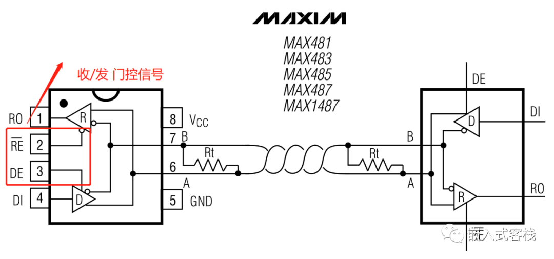
When the Host sends data, the data travels along the red line through twisted pairs to the differential receiving circuit of the Slave. When the Slave responds, the data travels in the blue direction to the Host’s receiving circuit. However, since the transmission medium is a pair of twisted pairs, one side cannot transmit signals while transmitting data. From the perspective of the transceiver’s control:On the control chip side, a GPIO pin is used to control the transceiver enable, making it easy to understand through a chip internal principle block diagram:
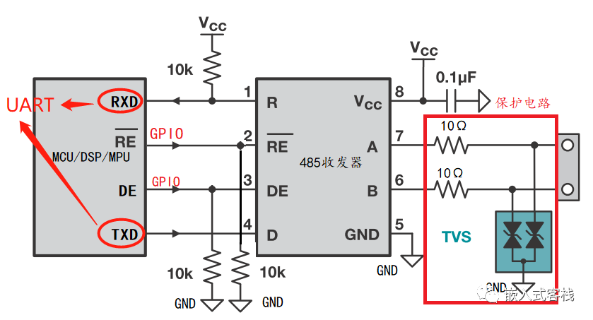
When DIR=0, the receiving circuit is enabled, and the transmitting circuit is disabled DE=0, which is equivalent to high impedance for the bus; when DIR=1, the receiving circuit is enabled, and the transmitting circuit is disabled DE=1, which depends on the signal of DI for the A/B signals of the bus. Here are two questions:1. Why does the chip design as opposite effective logic? This is also convenient for using a GPIO to control the transceiver circuit.2. Why not make the transceiver chip’s transceiver enable as one pin? For example, just call it DIR? It could also be made into two pins for separate control of send/receive, for example :
It is even possible to set it to 0 when DE=1, so can it self-loop? This can be designed in products, allowing for self-diagnosis of the transceiver and wiring by comparing received messages with sent messages to diagnose chip soldering, transceiver damage or disconnection, and wiring short-circuit faults.Perhaps you will say, nonsense! You just said RS-485 cannot send and receive simultaneously, but here you say it can self-loop, isn’t that contradictory? It is not contradictory; the previous statement about not being able to send and receive simultaneously refers to not being able to receive messages sent from other devices while sending.
Therefore, the essence of half-duplex is that the communication medium does not have a bidirectional channel. While sending data to the bus, the medium is occupied, and even if you want to send, you cannot correctly send the signal to the medium. If forced to send, data will be distorted, and the transceiver chip may be damaged.
The DIR pin in the diagram controls whether the current RS-485 is in “receive” or “send” mode.
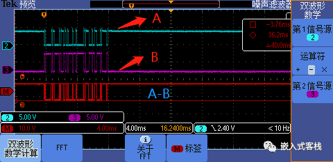
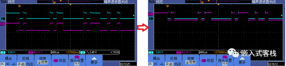
Earlier, we discussed common mode voltage indicators and differential mode transmission; let’s take a look at the waveform:The oscilloscope’s CH2 connects to the 485 output A end, CH3 connects to the 485 output A end, and the red line is the oscilloscope’s MATH function: CH2-CH3. Most oscilloscopes have mathematical operation functions.If you want to see the differential signal, a dual-channel oscilloscope with MATH subtraction function can be used. If some oscilloscopes do not have the MATH function, there is a trick:Inverting the negative end of channel B, or the differential signal, and then shifting channel B to overlap with the idle level can also intuitively show A-B?From this diagram, what valuable signal characteristics can be discovered?
Signal A is high when idle; signal B is low when idle. Therefore, you will see that some devices are labeled 485_A+ and 485_B-.
Each channel’s common mode voltage value is within the standard requirement of -7 to 12V, signal A is 4V, and signal B is 5V:
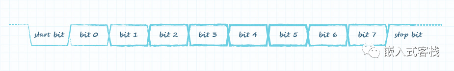
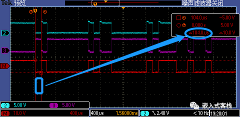
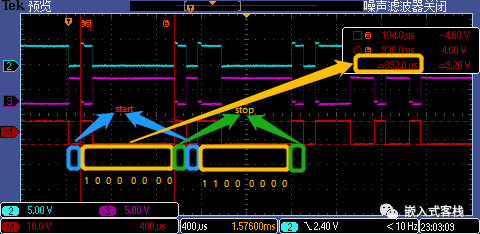
So how to interpret the data?The captured data is a MODBUS-RTU master sending a message to the slave device, the content of which is the first two bytes 0x01 0x03. The UART mode has 1 start bit, 8 data bits, 1 stop bit, no parity, and low bit first. This example UART communication format isFirst, calculate a few parameters based on the UART communication mode, such as bit time and byte time:This diagram shows that the width of the start bit is exactly 104us.For parsing this asynchronous serial timing waveform, the most important thing is to calculate bit time and byte time based on the communication format, and then directly parse the waveform data. From this perspective, if you want to use FPGA to implement a UART protocol logic analyzer, this is the core indicator. Let me act as a visual UART logic analyzer:The time width of the 8-bit data is exactly 832us. Since the format is low bit first, it needs to be reversed to match the actual sent data 0x01 0x03.When debugging the lower level, this method can be used to check whether the software correctly drives the hardware. For example, when debugging I2C/SPI and other lower-level interfaces, similar methods can be used to check hardware waveforms. The only difference is that I2C/SPI belongs to synchronous communication, which means that its communication layer has a synchronous clock signal; I2C’s SCL and SPI’s SCK are synchronous clocks.
Driving Capability
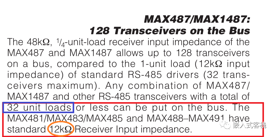
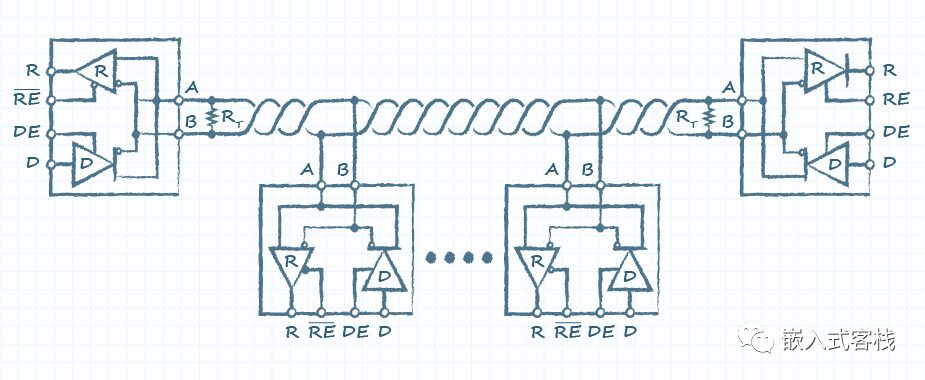
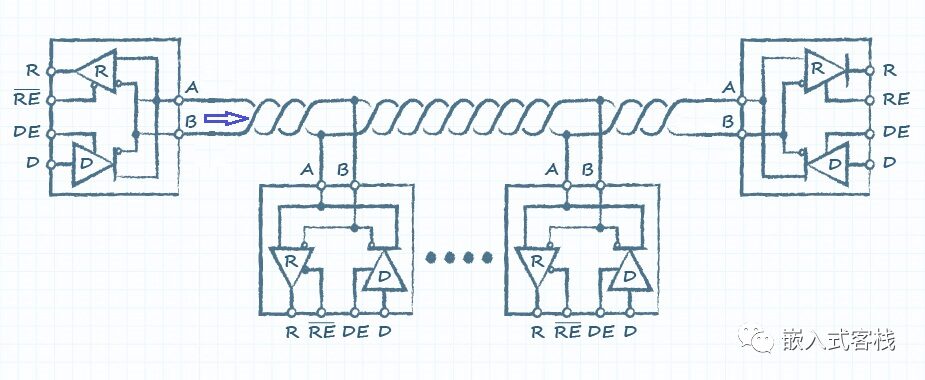
The electrical parameters summarize that the maximum electrical driving capability of RS-485 can drive up to 32 stations under multipoint network topology structure. How should this metric be interpreted?First, let’s examine the characteristics of a station’s transceiver circuit. The standard equivalent input impedance of the receiver circuit of the transceiver is 12kΩ. For example, take the MAX 485 data sheet as an example:Why 32? Mainly due to the previous stipulation of a minimum driving capability of 200mV.It can also be understood this way: each receiver circuit input impedance is not an ideal high impedance but 12kΩ. For example, if one station sends, it is equivalent to having 32 stations’ input impedances in parallel. Why 32? Don’t forget that the sending station itself also has a receiving circuit, so not considering termination resistance and line impedance, the sending circuit is connected to an equivalent load: and the sending circuit’s driving capability is certainly limited, making it easier to understand.The diagram below illustrates what is known as multipoint network topology, where all stations are arranged along the twisted pair and connected to the bus.Therefore, you may see the term “RS-485 unit load” in some places. Here, the so-called unit load refers to the 12kΩ standard input impedance, which is defined by the EIA-485 standard. Thus, terms like unit load originate from this.
Data Monitoring
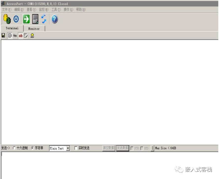
For example, in an RS-485 based Modbus-RTU multipoint network, when doing protocol programming or debugging the actual multi-station bus, it may be necessary to monitor all messages on the bus. It is even possible to implement a bus message recorder that records all messages on the bus. How to achieve this?Buy a USB to RS-485 converter cable or make one yourself. Connect the A/B lines to the bus, plug the USB into the computer. Use a serial port monitoring terminal or write a small software to receive serial data, and you can monitor all messages on the bus.For example, this AccessPort serial tool is quite useful:
Application Design
In application design, these dimensions need to be considered:
Termination Design
Interface Chip
Isolation Design
Termination Design
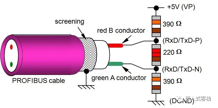
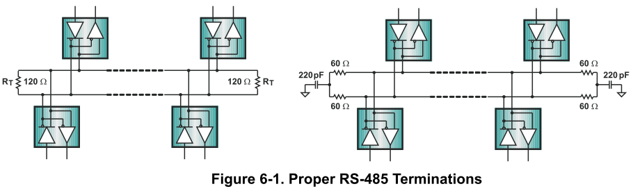
First, why is termination necessary? This is because RS-485 uses twisted pair transmission, and the standard specifies that the differential characteristic impedance of twisted pairs is between 100Ω and 150Ω. The standard RS-485 creators chose 120Ω as the nominal characteristic impedance.Assuming the signal is sent out from the left station, if there is no termination, the signal will have continuous impedance during transmission on the line, but when it reaches the right side, the equivalent impedance becomes the input impedance of the receiving circuit, for example, 12kΩ. The impedance is no longer continuous, leading to impedance discontinuity! A portion of the signal energy will return along the original path, and the reflected signal will interfere with the original signal due to capacitance and inductance, causing communication errors. In severe cases, communication may fail completely.To understand the underlying principles more deeply, you can study transmission line theory.Perhaps friends who have worked with Profibus DP (which also uses RS-485 as the physical layer) might say, look at why the recommended termination circuit for Profibus DP is as follows?This is because the communication medium used in Profibus DP has different nominal characteristic impedance. Therefore, there will be slight differences in actual engineering applications.In TI’s documentation, there is a termination method:In environments with significant noise, it is recommended to use the termination scheme on the right, utilizing two 60Ω resistors and a 220pF capacitor to form a low-pass filter, thereby increasing the line’s noise immunity.When wiring in actual engineering, if encountering significant noise, one can use an oscilloscope to check the bus signal quality and make slight adjustments to the termination method.
Interface Design
Many chip manufacturers provide RS-485 transceiver chips, such as TI, Microchip, etc. When choosing an interface chip, consider whether the chip’s power supply voltage input logic is compatible with the logic levels of the microcontroller/DSP being used. Additionally, check whether the input impedance of the receiving circuit conforms to the RS-485 standard input impedance. If not, the number of loads that can be supported during network deployment may need to be adjusted. Also, note that some new designs of RS-485 transceivers have fail-safe functions.Furthermore, as mentioned earlier, standard transceivers can drive up to 32 standard transceiver load devices, meaning (12kΩ) standard unit input impedance.When designing specific interface circuits, EMC requirements must also be considered. In some field devices, strong interference may occur, such as large inductive devices running on the power line. Additionally, there may be space radiation interference. In such cases, consider using shielded twisted pairs, connecting the shield to ground. My understanding of anti-interference is not very deep; I just summarize it. Here, I found a lightning protection interface circuit design scheme that can be referenced:https://www.programmersought.com/article/95833359295/Earlier, it was mentioned that standard RS-485 can accommodate 32 standard receiving impedance transceiver devices. If you want to connect more than 32 station devices in an actual system, what should you do? You can design a relay device. This is akin to connecting two network segments using a relay to solve the problem of insufficient driving capability. There are also ready-made products available for this.
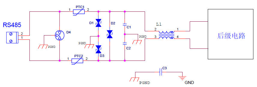
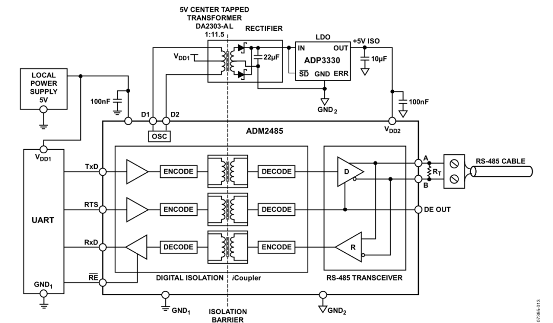
Isolation Design
Why is isolation necessary? To reduce ground noise. In many fields, there may be large current switching devices, inductive devices, etc., and noise may couple into the equipment through communication grounding. Especially in industrial equipment, interfaces are generally designed to include isolation. To design an isolated interface, consider choosing chips with isolation functions, such as ADI’s iCoupler technology products ADM2481, ADM2485. Alternatively, a combination of optocouplers and standard RS-485 transceivers can also be used. The only thing to note is that it is necessary to design an isolated power supply to power the circuits on both sides of the isolation.The above diagram is from TI’s “The RS-485 Design Guide,” which is a very good document, and many parts of this article were organized based on this document. If you are interested in this document, you can reply with 485 in the background to receive it automatically.
In Summary
RS-485 may seem simple, but there are many things to understand and pay attention to when designing applications. To create a robust product, often the difference is not in the big direction, but in small details that can easily lead to product instability.References: TI: The RS-485 Design Guide
1. Sign up! Building a secure embedded system–From FreeRTOS to SAFERTOS online course
2. The 6th issue of the 2021 “Microcontroller and Embedded System Applications” electronic journal is freshly out!
3. Huawei’s official notification: Harmony no longer belongs to Huawei!
4. Clever use of MCU’s universal registers that do not reset SystemReset!
5. With such limited resources in microcontrollers, why do so many people want to use RTOS?
6. On Children’s Day, reminiscing about the university days obsessed with technology!
Disclaimer: This article is a network reprint, and the copyright belongs to the original author. If there are any copyright issues, please contact us, and we will confirm the copyright based on the copyright certificate you provide and pay the remuneration or delete the content.